
Sputtering Targets
Sputtering targets are essential materials for magnetron sputtering, RF sputtering, DC sputtering and other vacuum thin-film deposition processes. Their chemical composition, purity, density, dimensions and backing configuration directly influence film composition, deposition stability, uniformity, adhesion and final performance.
This category covers a broad range of sputtering target systems, from high-purity elemental metals to binary alloys and advanced compounds. These materials support semiconductor, display, optoelectronic, photovoltaic, magnetic, sensor, decorative, wear-resistant, conductive and transparent-conductive thin-film applications.
Target selection should be matched to the desired film composition, deposition equipment, substrate dimensions and process conditions. Important purchasing parameters include material chemistry, purity, target geometry, dimensions, thickness, backing plate, bonding method and DC or RF compatibility.
Show More: Select Sputtering Targets by Material System
Material Systems and Application Areas
| Material system | Typical materials | Common application directions |
|---|---|---|
| High-purity elemental metals | Aluminum, copper, titanium, chromium, nickel, cobalt, silicon, tin, zinc, silver, gold and platinum | Conductive layers, metallic films, seed layers, barrier layers and functional electrodes |
| Refractory metals | Tungsten, molybdenum, tantalum, niobium, hafnium, vanadium and zirconium | High-temperature films, diffusion barriers, wear-resistant coatings and electronic devices |
| Alloy targets | Al-based, Ti-based, Ni-based, Co-based, Fe-based, Cu-based, Cr-based and refractory-metal alloys | Controlled alloy films and composition-specific thin-film development |
| Precious-metal and specialty alloys | Gold, silver, platinum, palladium and related alloy systems | Optical, electrical, catalytic, sensor and advanced-device films |
| Oxide targets | ITO, IZO, AZO, aluminum oxide, zinc oxide, titanium oxide and niobium oxide | Transparent conductive films, optical films, insulating layers and dielectric coatings |
| Nitride targets | Titanium nitride, aluminum nitride, silicon nitride, chromium nitride and related nitrides | Hard coatings, wear-resistant layers, decorative coatings, electronic and optical films |
| Carbide and boride targets | Titanium carbide, silicon carbide, tungsten carbide, titanium boride and zirconium boride | High-hardness, high-temperature, corrosion-resistant and wear-resistant coatings |
| Chalcogenide compound targets | Sulfides, selenides, tellurides and related multicomponent compounds | Photovoltaic, optoelectronic, thermoelectric, memory and semiconductor research |
| Phosphide, arsenide and specialty compounds | Phosphides, arsenides, antimonides and other multicomponent compounds | Compound semiconductors, infrared optoelectronics and advanced functional films |
| Magnetic and rare-earth materials | Ferromagnetic, soft-magnetic, rare-earth and magnetic alloy systems | Magnetic recording, magnetic sensors, magnetoelectric devices and spintronic research |
Geometry, Dimensions and Backing
Sputtering targets may be supplied as round, planar, rectangular, strip, rotary or custom-shaped formats, depending on the cathode and deposition system. Common specifications include:
- Material name, chemical formula and alloy composition;
- Purity grade and impurity-control requirements;
- Target diameter, length, width and thickness;
- Density, grain structure and surface condition;
- Copper or other backing-plate requirements;
- Indium bonding, elastomer bonding or other bonding options;
- DC, RF, pulsed-DC or reactive-sputtering compatibility;
- Substrate size, deposition area and mounting configuration.
For large-area coating, continuous deposition or special chamber configurations, target utilization, cooling, mounting interfaces and usable erosion depth should be confirmed before ordering.
Purity and Composition Selection
High-purity metal targets are commonly selected when film resistivity, optical properties, device reliability or contamination control is important. Alloy targets are used for stable multi-element film composition, while ceramic and compound targets support transparent conductive, dielectric, semiconductor, hard-coating and optical-film development.
When comparing targets, confirm the purity grade, impurity limits, composition basis, density, target structure and required documentation. Alloy ratios should be checked carefully because atomic percent and weight percent are not interchangeable.
Process and Application Directions
| Deposition route | Suitable target direction |
|---|---|
| DC magnetron sputtering | Conductive elemental metals and many alloy targets |
| RF sputtering | Insulating oxides, nitrides, ceramics and other compound targets |
| Reactive sputtering | Metal targets combined with oxygen, nitrogen or other reactive gases |
| Pulsed-DC sputtering | Processes requiring improved stability and reduced arcing |
| Co-sputtering | Composition screening and precise multi-element film adjustment |
Applications may include conductive films, transparent conductive films, semiconductor layers, dielectric coatings, barrier layers, magnetic films, optical coatings, hard coatings, wear-resistant coatings, decorative films and photovoltaic thin films.
Sputtering Target Selection Checklist
- What film chemistry or alloy composition is required?
- Is the composition specified in atomic percent or weight percent?
- What purity grade and impurity limits are acceptable?
- What target geometry and dimensions fit the cathode?
- Is a backing plate or bonded configuration required?
- Will the process use DC, RF, pulsed DC or reactive sputtering?
- What substrate size, deposition area and cooling conditions apply?
- Are composition analysis, certificates or other documents required?
Frequently Asked Questions
What types of sputtering targets are available?
Sputtering targets are available in elemental metal, alloy, oxide, nitride, carbide, boride, chalcogenide, semiconductor, magnetic and other specialty compound systems.
How do I choose between an elemental and an alloy target?
Choose an elemental target for a single-material film or a co-sputtering process. Choose an alloy target when a defined multi-element composition is required from one sputtering source.
Is higher purity always better?
Higher purity can reduce contamination and support demanding electrical, optical or semiconductor applications, but the appropriate grade depends on the film specification, equipment and budget.
Do sputtering targets require a backing plate?
The requirement depends on target size, cathode design, cooling method and operating power. Confirm the mounting and bonding configuration with the deposition-system requirements.
How do I choose a round, planar or rectangular target?
Match the target geometry to the cathode and fixture. The required diameter, length, width and thickness should be confirmed before placing an order.
Can insulating materials be sputtered?
Yes. Oxide, nitride and other insulating compound targets are commonly processed by RF sputtering. The final choice depends on the target material and equipment configuration.
Can target composition and dimensions be customized?
Special alloy ratios, compound compositions, non-standard dimensions, backing plates and bonding configurations may be available for specific process requirements.
What information should be included in an inquiry?
Include the material or chemical formula, purity, alloy ratio, target geometry, dimensions, thickness, backing or bonding requirements, sputtering method, quantity and any required material documentation.
Showing 81–96 of 148 results
-
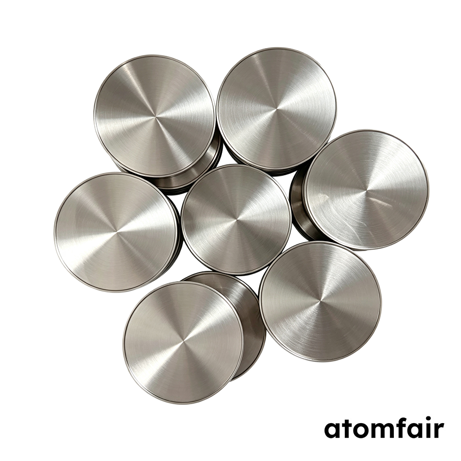
NbTi Sputtering Target 99.9% 2in Research ATOMFAIR®
$510.00 -
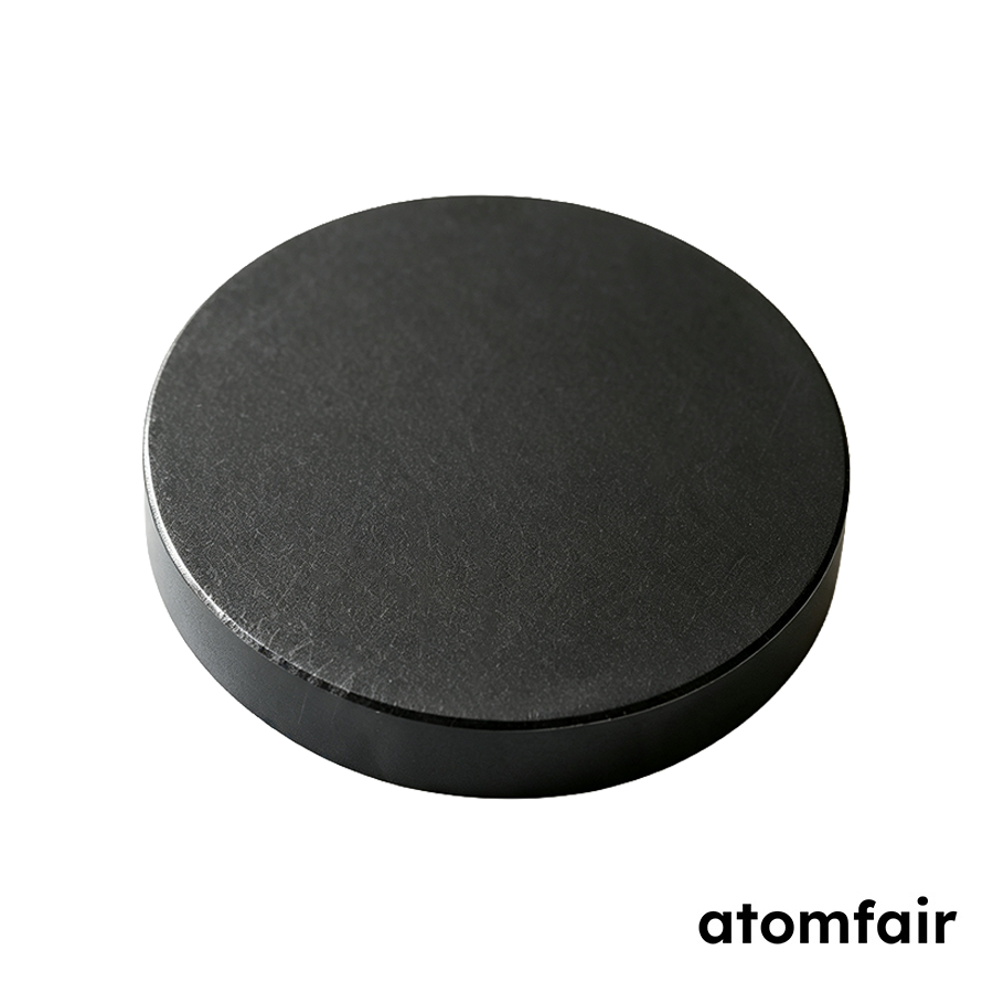
Nd2Fe14B Sputtering Target 99.95% 3in x 0.125in ATOMFAIR®
$690.00 -
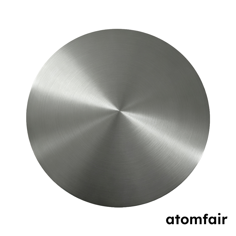
Nickel-Aluminum Sputtering Target 2 in 99.95% ATOMFAIR®
$395.00 -
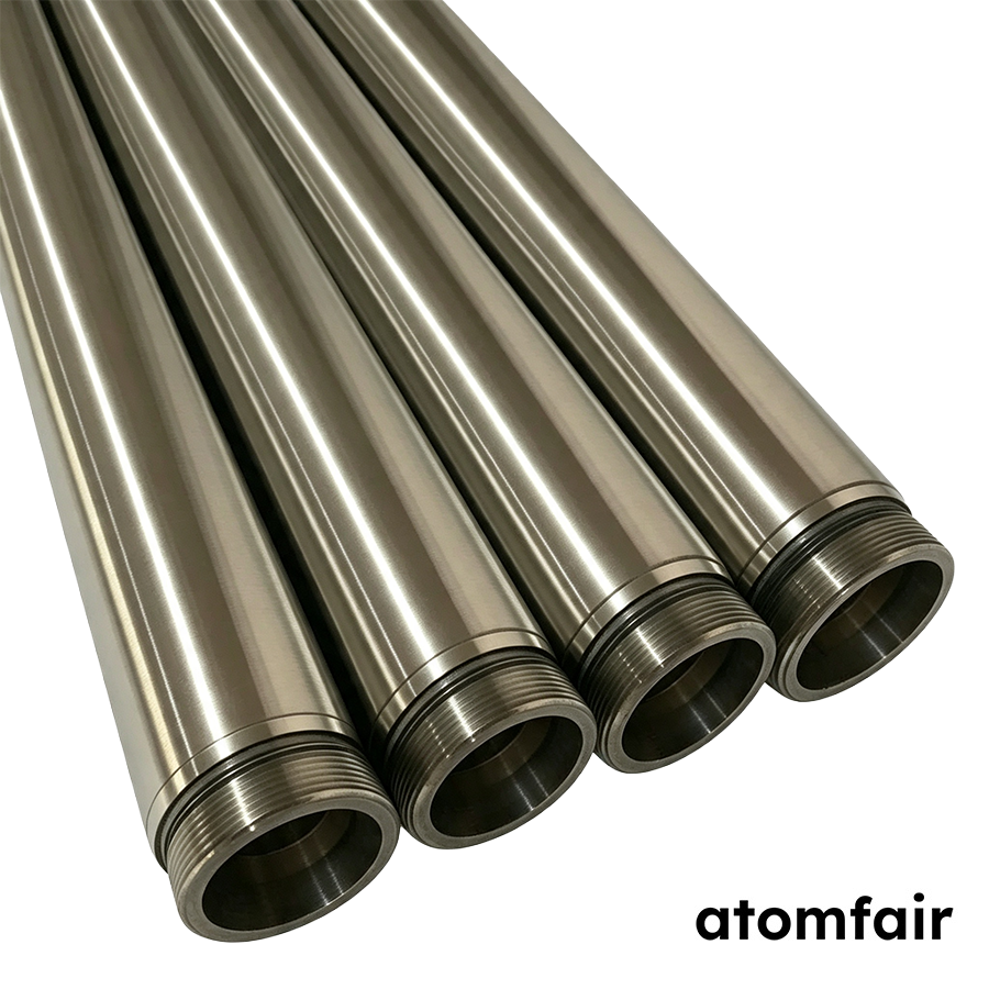
Nickel-Chromium Sputtering Target 99.5% NiCr ATOMFAIR®
$510.00 -
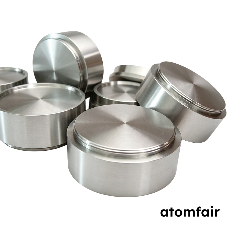
Nickel-Iron Alloy Sputtering Target 99.9% 2in ATOMFAIR®
$230.00 -
Nickel-Molybdenum-Tungsten Sputtering Target 99.9% ATOMFAIR®
$230.00 -
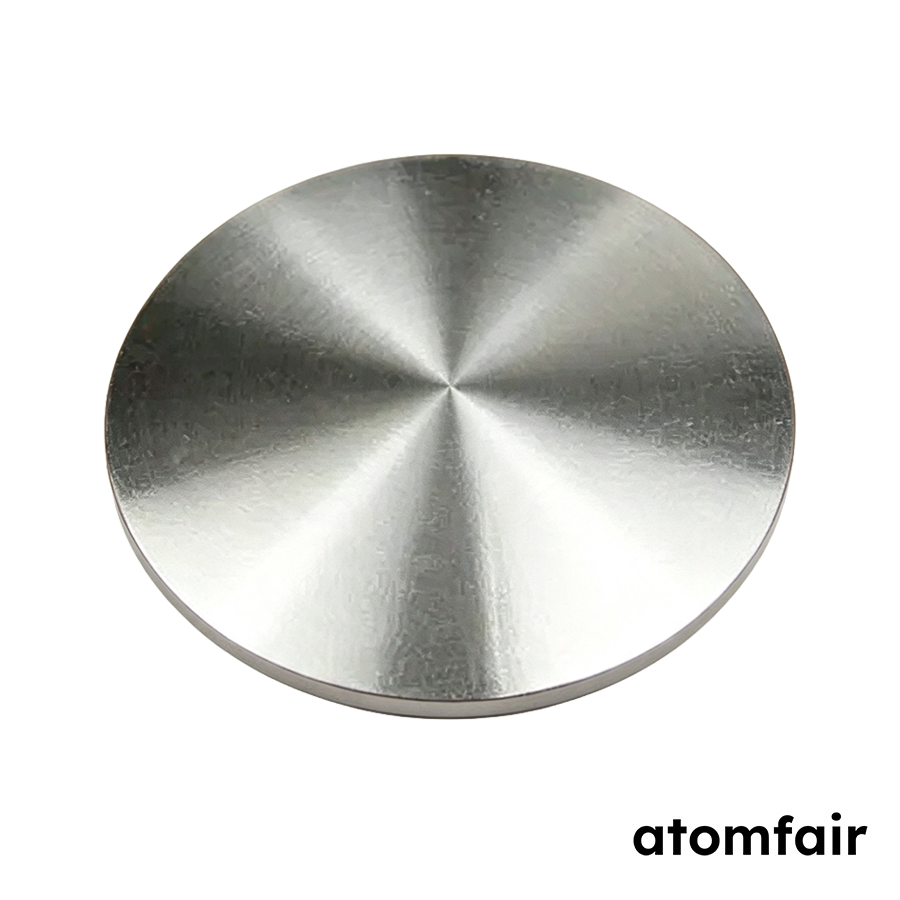
Nickel-Niobium-Tantalum Sputtering Target 3in×3mm ATOMFAIR®
$620.00 -
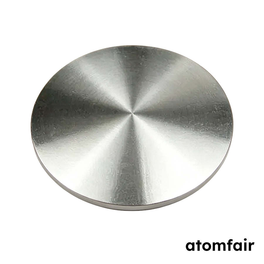
Nickel-Platinum Sputtering Target 3 in x 0.125 in ATOMFAIR®
$460.00 -
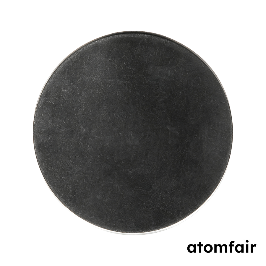
Nickel-Silicon NiSi Sputtering Target 99.5% 2 in ATOMFAIR®
$225.00 -
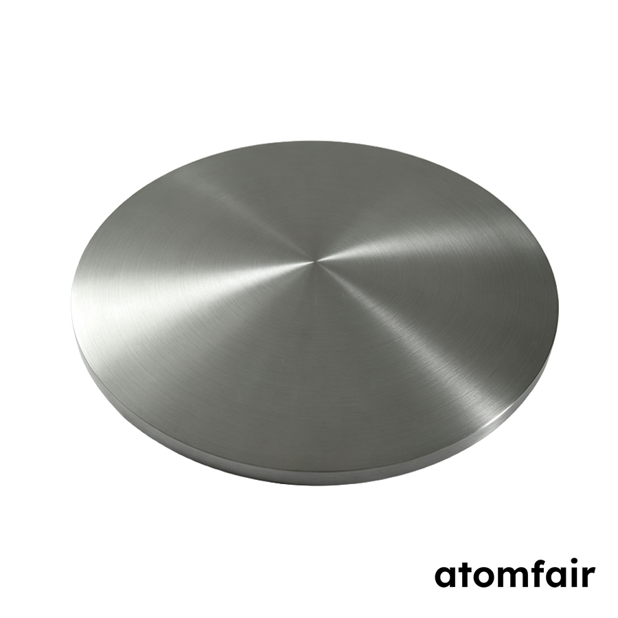
Nickel-Tungsten Alloy Sputtering Target 99.9% ATOMFAIR®
$230.00 -
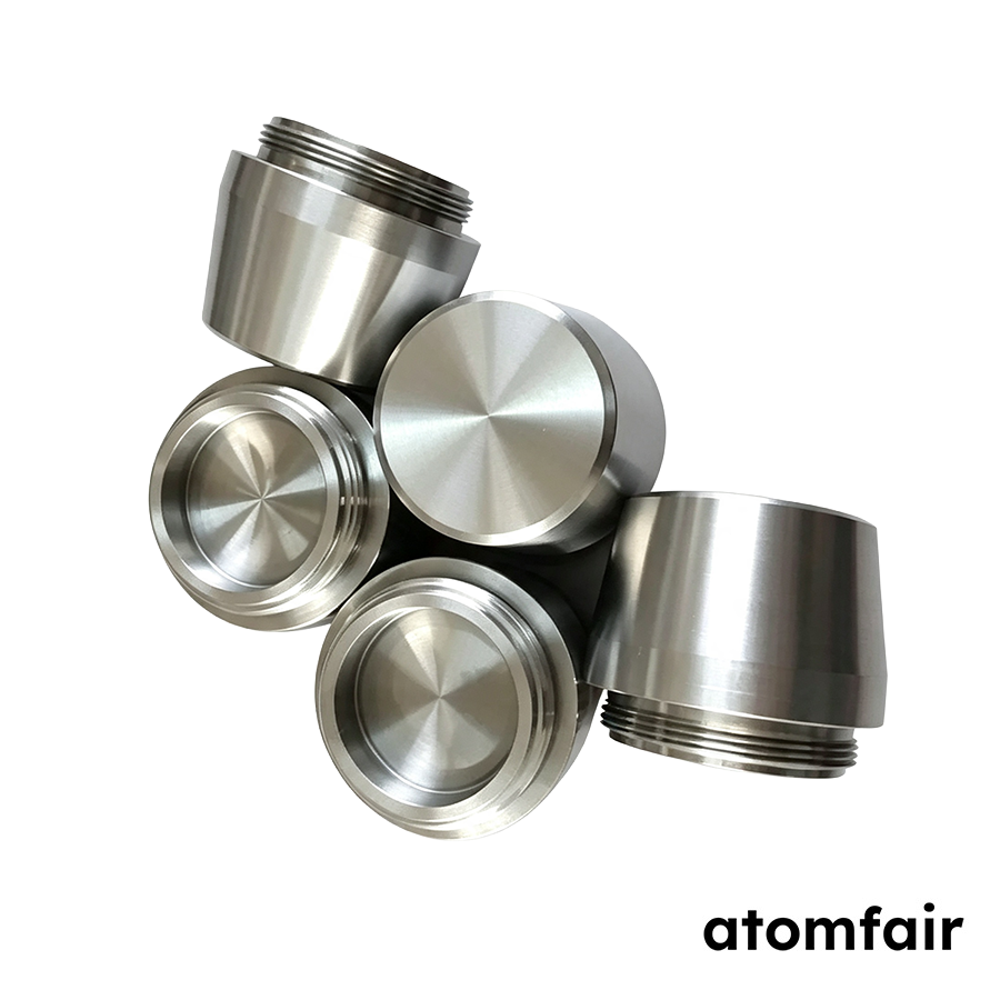
Nickel-Vanadium Alloy Sputtering Target 99.95% ATOMFAIR®
$240.00 -
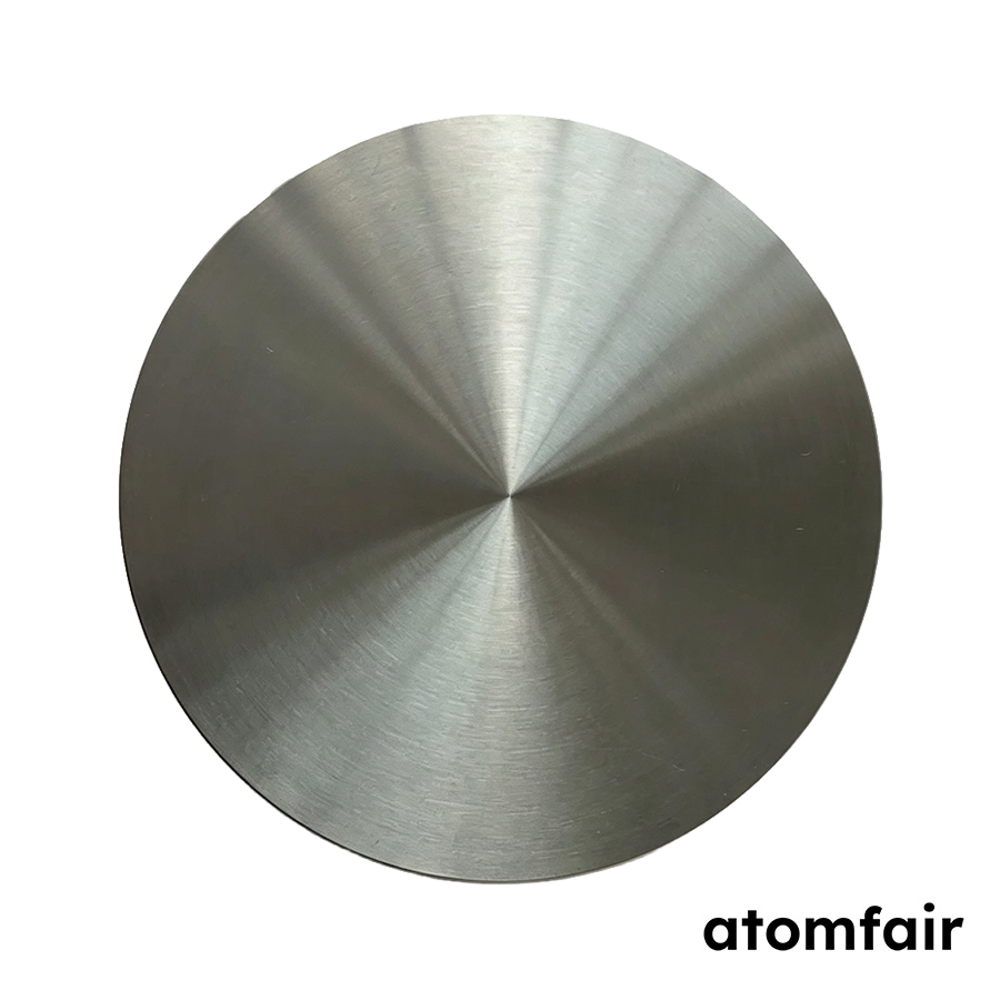
NiCr 80:20 Sputtering Target 99.95% 3 in Lab ATOMFAIR®
$645.00 -
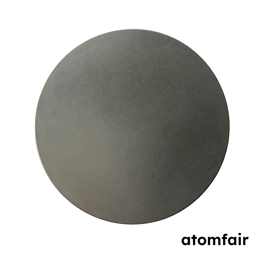
NiCrFe (72:14:14) Alloy Sputtering Target 99.95% ATOMFAIR®
$960.00 -
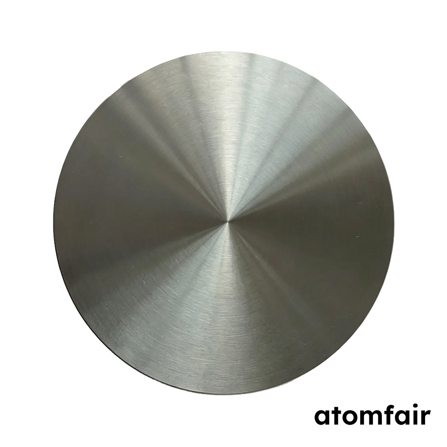
NiCuMn Alloy Sputtering Target 99.9% 3 in ATOMFAIR®
$445.00 -
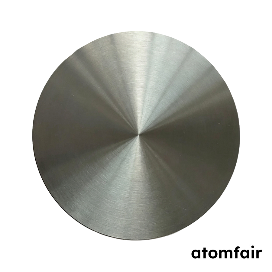
NiMn(50:50 at%) Alloy Sputtering Target 99.95% ATOMFAIR®
$240.00 -
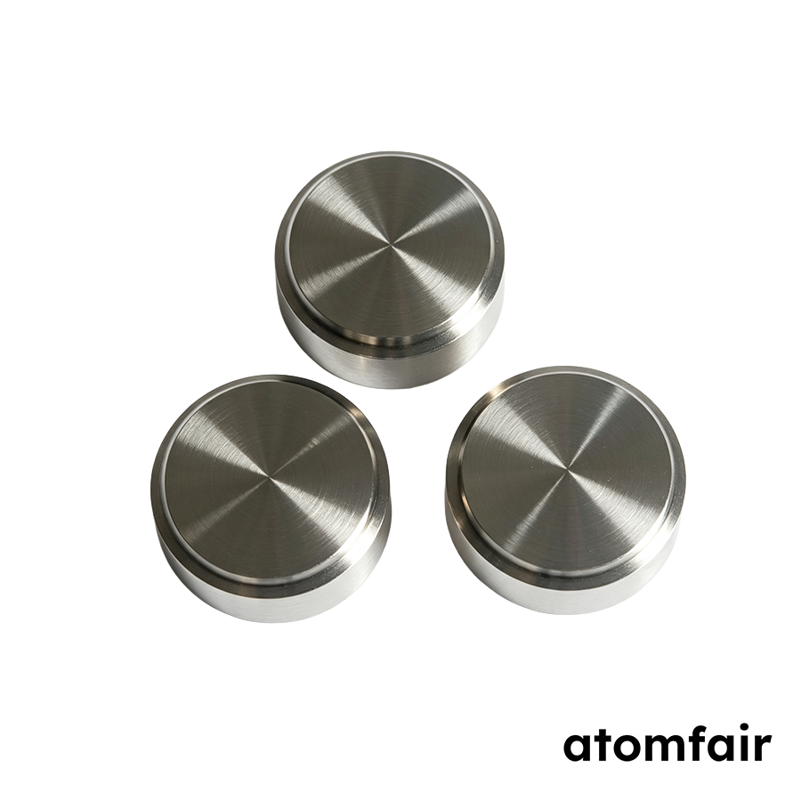
NiMo Alloy Sputtering Target 99.95% 2-inch ATOMFAIR®
$240.00