|
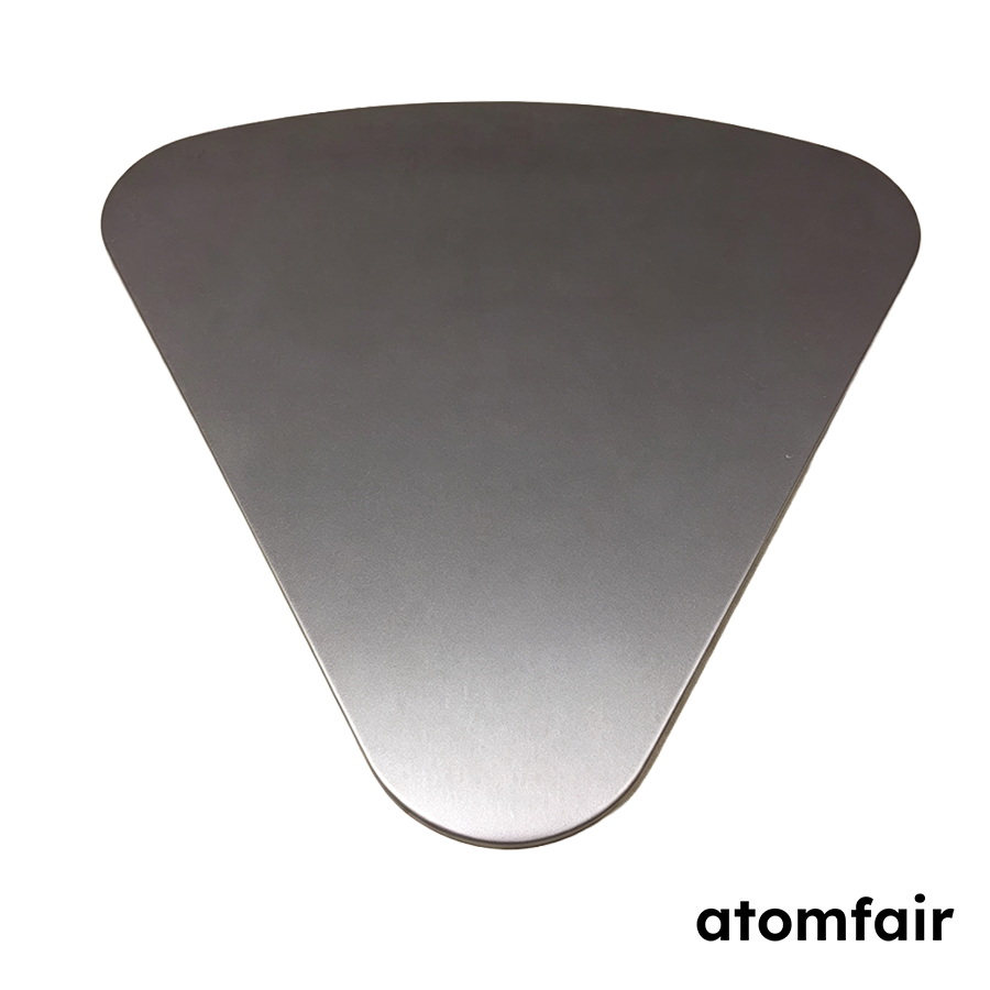
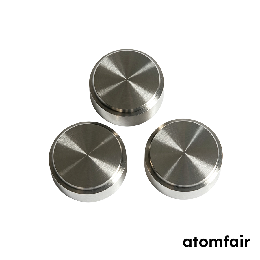
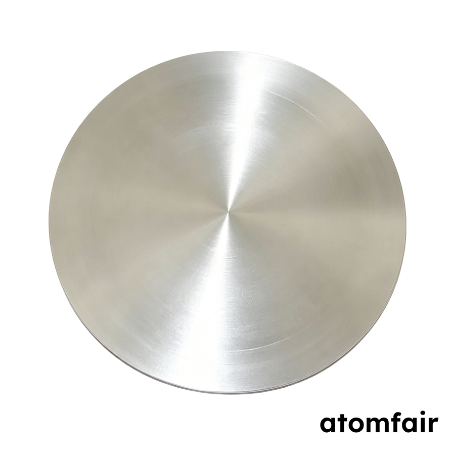
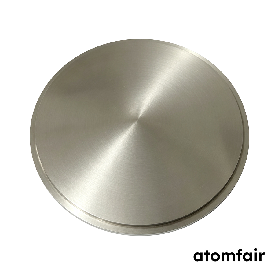
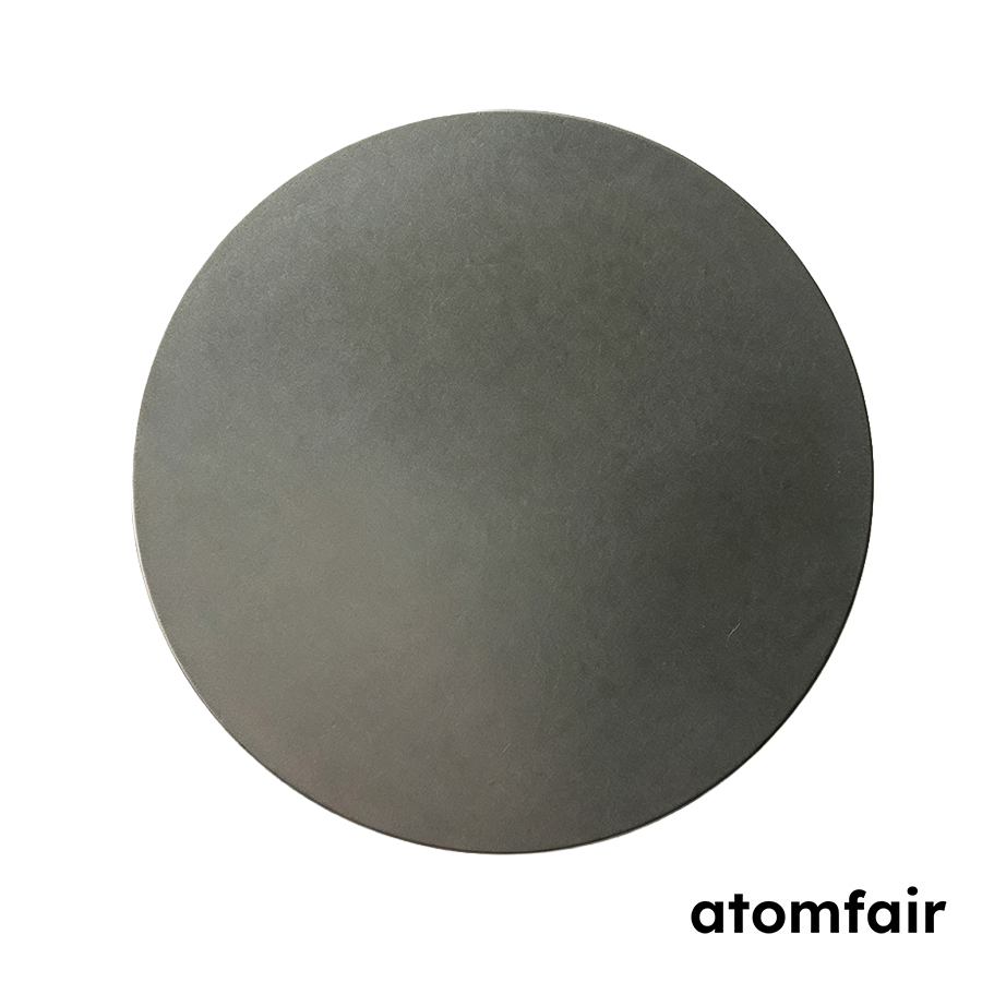
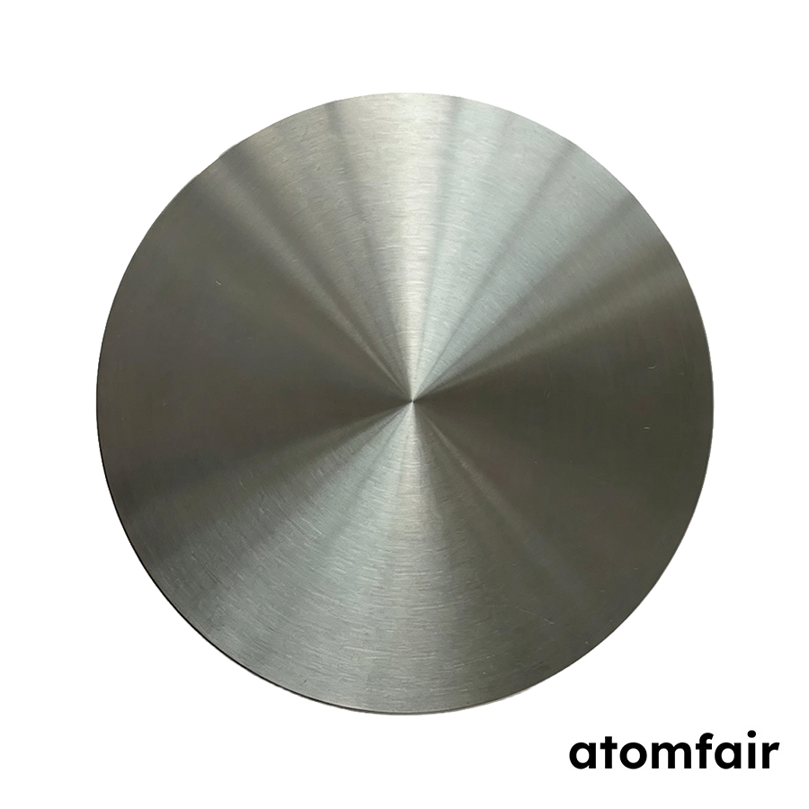
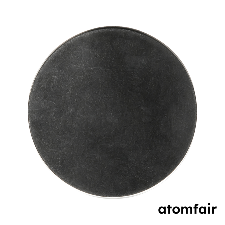
Nickel-Silicon Alloy Sputtering Target (NiSi)
Product Type: Metal alloy sputtering target
Research-grade laboratory product
|
|||||||||||||||||||||||||||||||||||||
|
|||||||||||||||||||||||||||||||||||||
|
LABORATORY PROCUREMENT SUPPORT
INQUIRY: inquiry@atomfair.com
|
|||||||||||||||||||||||||||||||||||||
|
Manufacturer: Atomfair LLC
Brand: ATOMFAIR®
|
This document defines the technical constraints for integrating the ATOMFAIR NiSi sputtering target into vacuum deposition workflows. It is limited to processing, bonding, and substrate-related requirements stated for this product.
- Deposition process constraints: Operate the target by DC or RF magnetron sputtering under an argon atmosphere to maintain the stated deposition window.
- Power density limits: Apply DC power densities from 3 to 15 W/cm² or RF power densities from 1 to 5 W/cm² to avoid exceeding the rated target load.
- Pressure and uniformity: Maintain an argon pressure between 0.5 and 2.0 Pa to support the stated deposition rate and thickness uniformity across a 100 mm substrate.
- Bonding and backing plate compatibility: Select indium or elastomer bonding and an oxygen-free copper or CuCrZr backing plate that match the deposition system's mounting and cooling configuration.
- Substrate preparation: Prepare substrate surfaces to meet the stated adhesion strength requirement of greater than 15 MPa for deposited films.
This procedure covers target installation, vacuum chamber setup, and deposition initiation for the ATOMFAIR NiSi sputtering target. It is intended for research-scale DC/RF magnetron sputtering systems.
Required Equipment: Magnetron sputtering system with DC/RF power supply, Argon gas supply, Vacuum chamber, Substrate holder
- Confirm target specifications
Confirm the target composition, dimensions, purity, and bonding configuration match the deposition system's mounting and power requirements before installation. - Install target assembly
Install the bonded target assembly onto the magnetron cathode, ensuring the backing plate contacts the cooling surface. - Evacuate chamber
Close the vacuum chamber and evacuate it before introducing argon. - Set process conditions
Set the argon pressure to 0.5–2.0 Pa and apply DC or RF power within the rated density range for this target. - Start deposition
Start the deposition process and monitor the deposition rate and thickness uniformity across the substrate.
What are the optimal DC and RF magnetron sputtering parameters for achieving stoichiometric NiSi film transfer with the 99.5% purity target?
For stoichiometric NiSi deposition within ±2 at%, operate DC magnetron sputtering at 3-15 W/cm² or RF sputtering at 1-5 W/cm² under 0.5-2.0 Pa Ar atmosphere. This yields deposition rates of 10-80 nm/min with ±5% thickness uniformity across a 100 mm substrate, as specified in the product's technical parameters.
Which bonding type and backing plate options are available for the NiSi sputtering target, and how do they affect compatibility with different sputtering systems?
The target supports indium bonding or elastomer bonding (optional) with backing plates of oxygen-free copper or CuCrZr (optional). Indium bonding provides high thermal conductivity for high-power DC sputtering, while elastomer bonding is preferred for RF systems requiring lower thermal load. Backing plate material should match the system's cooling and clamping design; the product listing confirms these options.
What storage and handling requirements are recommended to preserve the NiSi target's pore-free structure and fine grain size for vacuum deposition?
The NiSi target has a relative density ≥95% of theoretical and a fine grain size ≤50 µm, making it sensitive to moisture and oxidation. Store in a dry, inert atmosphere (e.g., vacuum desiccator or argon-purged container) and handle with clean, powder-free gloves to avoid surface contamination. The machined surface finish (Ra ≤0.8 µm) should be preserved to maintain consistent sputter erosion.
The NiSi sputtering target (99.5% purity, ≤50 µm grain size) is optimized for DC/RF magnetron sputtering of thin-film resistors and diffusion barriers, delivering deposition rates of 10-80 nm/min with ±5% thickness uniformity. Its operational suitability depends on correct selection of bonding and backing plate options per the user's sputtering system.
Positive
- High-purity fine-grained NiSi alloy: 99.5% (2N5) purity with total metallic impurities <5000 ppm and O+N <1000 ppm, combined with ≤50 µm grain size, minimizes film contamination and supports consistent resistivity and adhesion in thin-film devices.
- Optimized sputtering performance: Specified for DC/RF magnetron sputtering at 3-15 W/cm² (DC) or 1-5 W/cm² (RF) under 0.5-2.0 Pa Ar, achieving deposition rates of 10-80 nm/min with ±5% thickness uniformity across a 100 mm substrate.
Trade-offs
- Bonding and backing plate dependency: The target requires selection of indium or elastomer bonding and an oxygen-free copper or CuCrZr backing plate, which must be matched to the user's sputtering system, adding integration complexity.
- Precise specification confirmation required: The buyer must independently verify target dimensions, composition ratio, purity, and bonding requirements against their deposition system before ordering, as the standard size (2 in diameter x 0.125 in) may not suit all systems.
Every advanced material, component, equipment, and instrument in our catalog is backed by rigorous testing. We maintain strict internal quality management frameworks and align with CE conformity metrics to deliver transparent, reproducible performance data via our public open-science repository.
To request raw batch performance data, submit formal vendor registration paperwork, or execute a fast-turnaround R&D manufacturing loop, contact us at inquiry@atomfair.com.
Item is dispatched under the Atomfair Shipping & Delivery Framework (Free worldwide shipping on orders over $59 USD excl. heavy equipment). Return is governed by the Atomfair Return & Refund Policy (7-day technical return window).