
Graphene-Like Materials
Graphene-Like Materials are an important group of advanced two-dimensional materials with layered structures, atomically thin characteristics, and tunable electrical, optical, thermal, mechanical, and chemical properties. Compared with conventional bulk materials, these materials often provide distinctive interlayer interactions and high surface activity for research in nanoelectronics, optoelectronics, energy materials, catalysis, sensing, composites, thin-film engineering, and fundamental materials science.
This category includes layered crystals, nanosheets, few-layer materials, ultrathin powders, liquid dispersions, thin films, and substrate-supported two-dimensional materials. Different material systems offer different combinations of conductivity, semiconducting behavior, insulation, optical response, magnetism, lubrication, chemical stability, and environmental sensitivity.
When selecting a material, first identify the required material system and physical form. Then compare the parameters relevant to the intended process, including purity, layer number, thickness, lateral size, particle size, concentration, solvent, substrate, sample area, and package size.
Show More: 2D Materials by Form, Material System, and Research Route
Main Types of Graphene-Like Materials
Transition Metal Dichalcogenides
Transition metal dichalcogenides are among the most widely studied graphene-like two-dimensional materials. This family includes sulfides, selenides, and tellurides with semiconducting, metallic, semimetallic, or phase-dependent properties. They are used in transistors, photodetectors, light-emitting devices, sensors, catalysts, batteries, and supercapacitors.
Common selection routes include:
- Semiconducting two-dimensional materials
- Metallic or semimetallic layered materials
- Monolayer, few-layer, and multilayer materials
- Powders, nanosheets, dispersions, and layered crystals
- Materials for device fabrication, composite systems, and catalytic research
Hexagonal Boron Nitride and Insulating 2D Materials
Hexagonal boron nitride has a layered structure similar to graphene while offering excellent insulation, thermal stability, and chemical stability. It can be used as an independent two-dimensional functional material or as a dielectric layer, protective layer, encapsulation layer, thermal-management material, and interface material in heterostructures.
Available selection directions may include:
- Hexagonal boron nitride crystals
- Monolayer or multilayer films
- Supported films on copper foil, nickel foil, or silicon-based substrates
- Materials for transfer, encapsulation, insulation, and interface engineering
Black Phosphorus, Violet Phosphorus, and Phosphorus-Based Layered Materials
Phosphorus-based two-dimensional materials have distinctive layered structures and anisotropic properties. They are studied in optoelectronics, electronics, sensing, energy materials, and fundamental materials research. Different thicknesses and physical forms can provide different band-gap, optical, and transport characteristics.
These materials can generally be selected by:
- Layered or bulk crystals
- Powders and nanosheets
- Few-layer or ultrathin materials
- Liquid dispersions
- Materials for optoelectronic devices, sensors, and heterostructures
Some phosphorus-based materials are sensitive to air, moisture, or light. Storage, transfer, packaging, and laboratory handling requirements should therefore be considered before purchase.
Layered Magnetic and Emerging 2D Crystals
Some layered materials exhibit magnetic behavior, antiferromagnetism, phase transitions, or strong interlayer coupling. These materials are relevant to spintronics, quantum materials, low-dimensional magnetism, phase-transition devices, and condensed-matter research.
When selecting layered crystal materials, consider:
- Material composition and crystal phase
- Crystal dimensions and usable area
- Sensitivity to air, moisture, and temperature
- Whether the material will be used for exfoliation, device fabrication, or spectroscopy
- Whether inert-environment storage and handling are required
2D Nanosheets, Few-Layer Materials, and Ultrafine Powders
Nanosheets and few-layer materials are suitable for composites, coatings, inks, catalysts, thermal materials, tribological systems, and solution-processing research. Compared with large layered crystals, powders and nanosheets are generally more convenient for mixing, dispersion, and scalable processing.
Important selection factors include:
- Lateral size or flake diameter
- Particle-size range
- Thickness and layer number
- Purity and impurity level
- Quantity and package size
- Compatibility with subsequent dispersion, coating, or composite processing
Particle size, flake diameter, and layer thickness describe different material characteristics and should not be treated as interchangeable specifications. For applications requiring controlled surface coverage, conductive networks, or optical response, lateral dimensions and layer number should be evaluated together.
2D Material Dispersions
Two-dimensional material dispersions are suitable for spray coating, spin coating, drop casting, blade coating, printing, composite blending, and other solution-based processes. Compared with dry powders, dispersions can simplify pre-processing and make it easier to control material concentration and usage.
When selecting a dispersion, compare:
- Material type
- Concentration
- Solvent system
- Nanosheet size and layer number
- Stabilizers or other additives
- Package volume
- Compatibility with the target substrate, resin, or formulation
For electronic, optical, catalytic, or biological research, confirm that the solvent and additives will not interfere with the intended performance or analytical method.
2D Films and Substrate-Supported Materials
Thin films and substrate-supported materials are suitable for device fabrication, heterostructures, surface modification, encapsulation, interface studies, and thin-film characterization. Compared with powders and dispersions, supported films provide a more defined sample geometry and processing boundary.
Before selection, confirm:
- Monolayer, few-layer, or multilayer structure
- Substrate material
- Film dimensions and usable area
- Whether transfer is required
- Surface condition and film continuity
- Compatibility with deposition, etching, encapsulation, and testing processes
Choosing the Right Material Form
First define the role of the material in the experiment or process: conductive layer, semiconductor, insulating layer, catalytic material, reinforcing filler, thermal material, or research crystal. Then select the form that best matches the workflow.
| Research or Processing Requirement | Material Forms to Consider |
|---|---|
| Mechanical exfoliation, crystal structure, and fundamental properties | Layered crystals and bulk crystals |
| Device fabrication and heterostructure research | Monolayer or multilayer films and substrate-supported materials |
| Coatings, inks, and composite materials | Nanosheets, few-layer powders, and dispersions |
| Catalysis and high-surface-area applications | Nanosheets, ultrafine powders, and liquid dispersions |
| Optoelectronics and sensing | Monolayer, few-layer materials, and high-quality films |
| Thermal management, lubrication, and reinforcement | Powders, flake materials, and composite-grade dispersions |
When comparing products, review the material type, purity, layer number, thickness, flake diameter, particle size, concentration, solvent, substrate, sample dimensions, and package quantity. For sensitive materials, confirm storage and handling requirements in advance.
Frequently Asked Questions
What is the difference between graphene and graphene-like materials?
Graphene is a two-dimensional material made of carbon atoms, while graphene-like materials are a broader group of layered two-dimensional materials. Their chemical composition, conductivity, band gap, magnetism, stability, and applications may be very different.
Should I choose a crystal, powder, or dispersion?
Choose a layered crystal when you need to perform exfoliation or study intrinsic crystal properties. Powders and nanosheets are generally more suitable for mixing, composites, and dry processing. Dispersions are convenient for coating, spraying, printing, and other solution-based processes.
What is the difference between monolayer, few-layer, and multilayer materials?
Layer number affects electrical, optical, mechanical, and surface properties. Monolayer materials are often selected for strong two-dimensional effects, few-layer materials balance two-dimensional behavior with easier handling, and multilayer materials are commonly used in powders, composites, coatings, and larger-scale processing.
Which is more important when selecting nanosheets: flake size or thickness?
They describe different properties. Flake size affects coverage, conductive networks, and composite structure, while thickness and layer number influence two-dimensional behavior, surface activity, and optical response. Both should be considered according to the intended application.
Can a two-dimensional material dispersion be used directly for coating?
Many dispersions can be used for coating, spraying, spin coating, or printing, but the result depends on the solvent, concentration, flake size, stability, substrate, and drying conditions. Confirm compatibility with the intended process and substrate before use.
What applications are suitable for hexagonal boron nitride?
Hexagonal boron nitride is commonly used for insulating layers, dielectric layers, encapsulation, thermal management, surface protection, and two-dimensional heterostructures. It is also available as a layered crystal for exfoliation and fundamental materials research.
Do phosphorus-based two-dimensional materials require special storage?
Some phosphorus-based two-dimensional materials are sensitive to air, moisture, light, or temperature and may require more careful storage and handling than stable oxide or sulfide materials. Review the material-specific packaging, storage, and laboratory handling requirements before purchase.
How can I select the right two-dimensional material for my application?
Define the required performance and processing method first, then compare the material system, product form, layer number, thickness, flake size, purity, solvent, substrate, and package quantity. For device, film, or sensitive-material applications, also confirm sample dimensions and process compatibility.
Showing 1–16 of 200 results
-
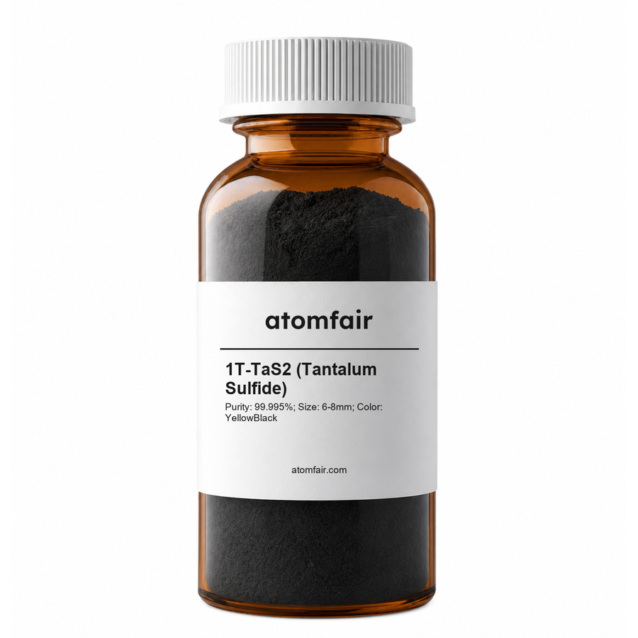
1T-TaS2 Tantalum Sulfide Crystal 99.995% 6–8mm ATOMFAIR®
$1,848.00 -
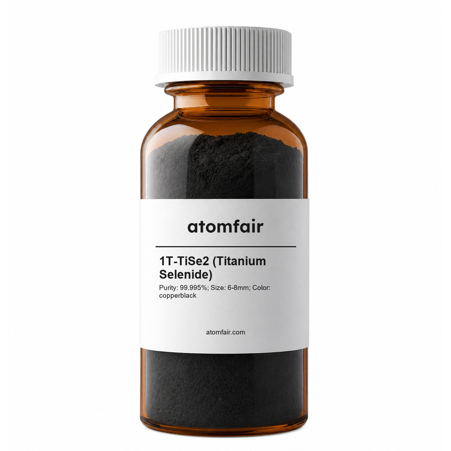
1T-TiSe2 Titanium Selenide Crystal 99.995% ATOMFAIR®
$1,848.00 -
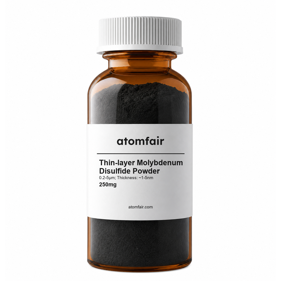
2D Molybdenum Disulfide Powder ~1–5nm 250mg ATOMFAIR®
$291.00 -
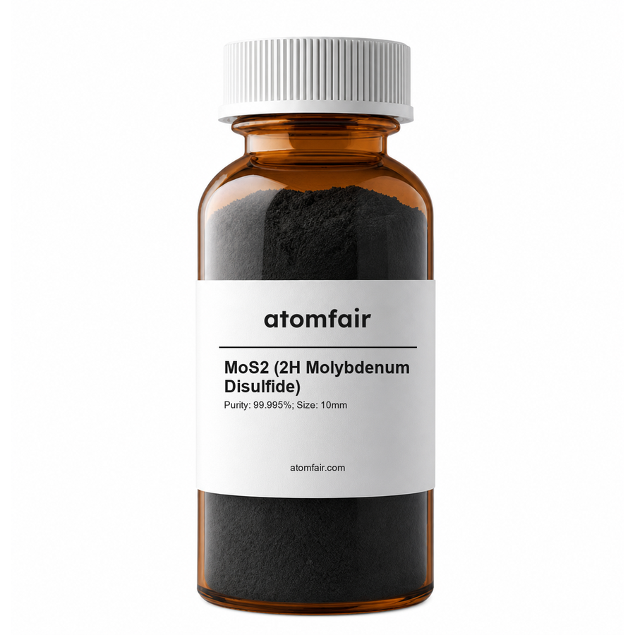
2H MoS2 Molybdenum Disulfide Crystal 99.995% ~10mm ATOMFAIR®
$1,848.00 -
2H-NbSe2 Crystal 99.995% ~8mm Black Gray Box ATOMFAIR®
$1,848.00 -
2H-Tantalum Selenide Crystal 99.995%, ~8mm ATOMFAIR®
$1,848.00 -
2H-TaS2 Tantalum Sulfide Crystal 99.995% 6–8mm ATOMFAIR®
$1,848.00 -
ACS Material CVD Hexagonal Boron Nitride >4μm 2.5cm×2.5cm
$566.00 -
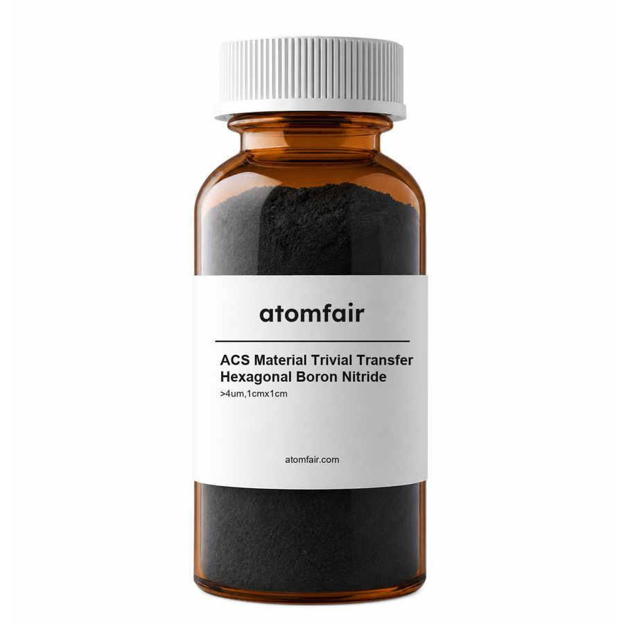
ACS Material hBN Trivial Transfer Film >4μm 1cm×1cm
$391.00 -
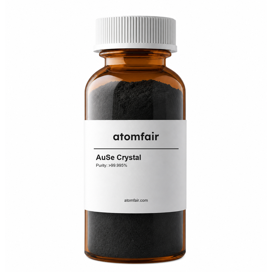
AuSe Crystal >99.995% Layered Research Grade ATOMFAIR®
$1,765.00 -
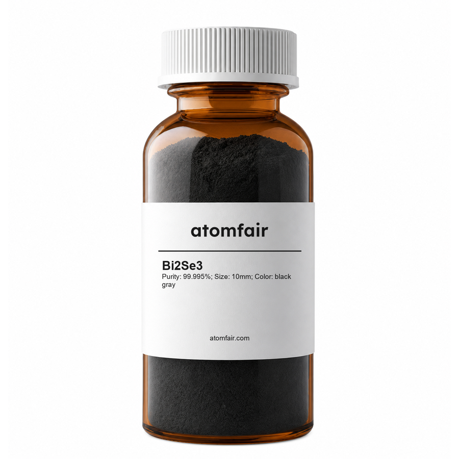
Bi2Se3 Layered Crystal Material 99.995% ~10mm ATOMFAIR®
$1,848.00 -
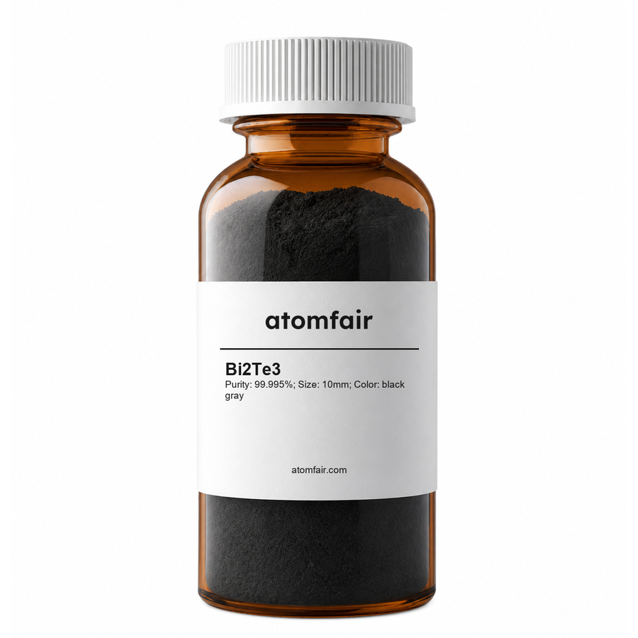
Bi2Te3 Layered Crystal Material 99.995% ~10mm ATOMFAIR®
$1,848.00 -
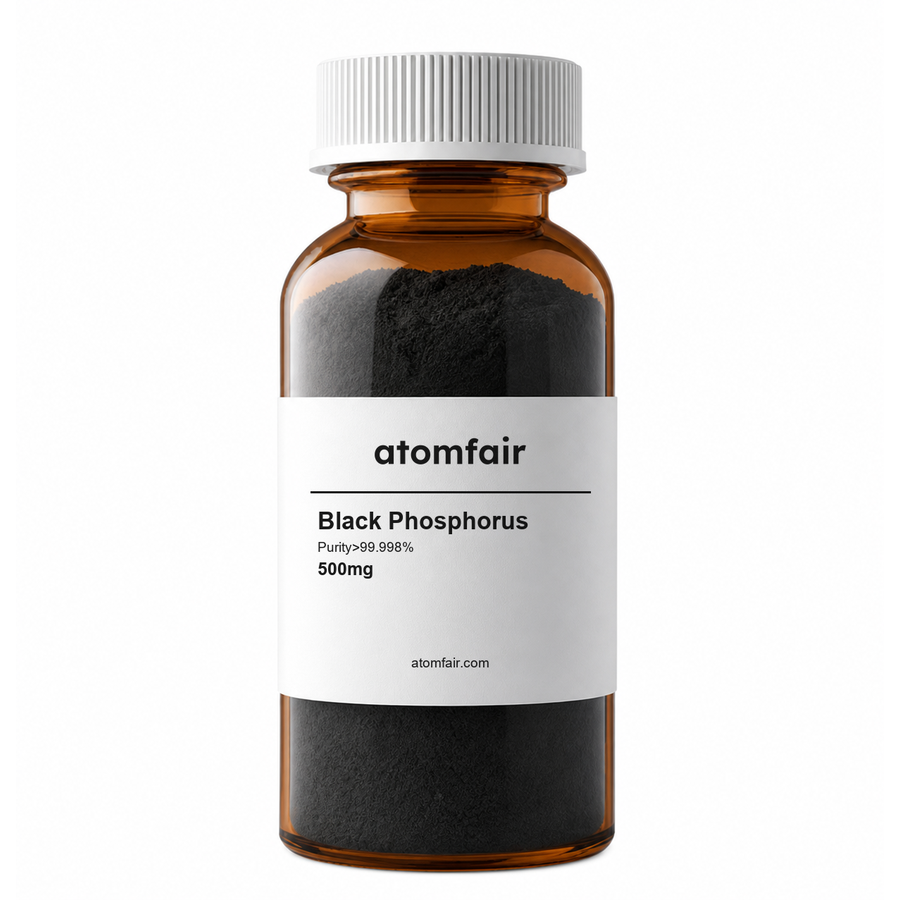
Black Phosphorus >99.998% 500mg Research Grade ATOMFAIR®
$566.00 -
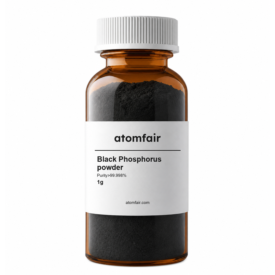
Black Phosphorus 2D Material Powder >99.998% 1g ATOMFAIR®
$1,405.00 -
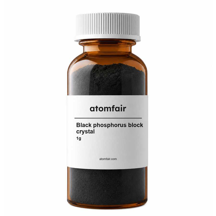
Black Phosphorus Block Crystal 1g, 1–10mm ATOMFAIR®
$364.00 -
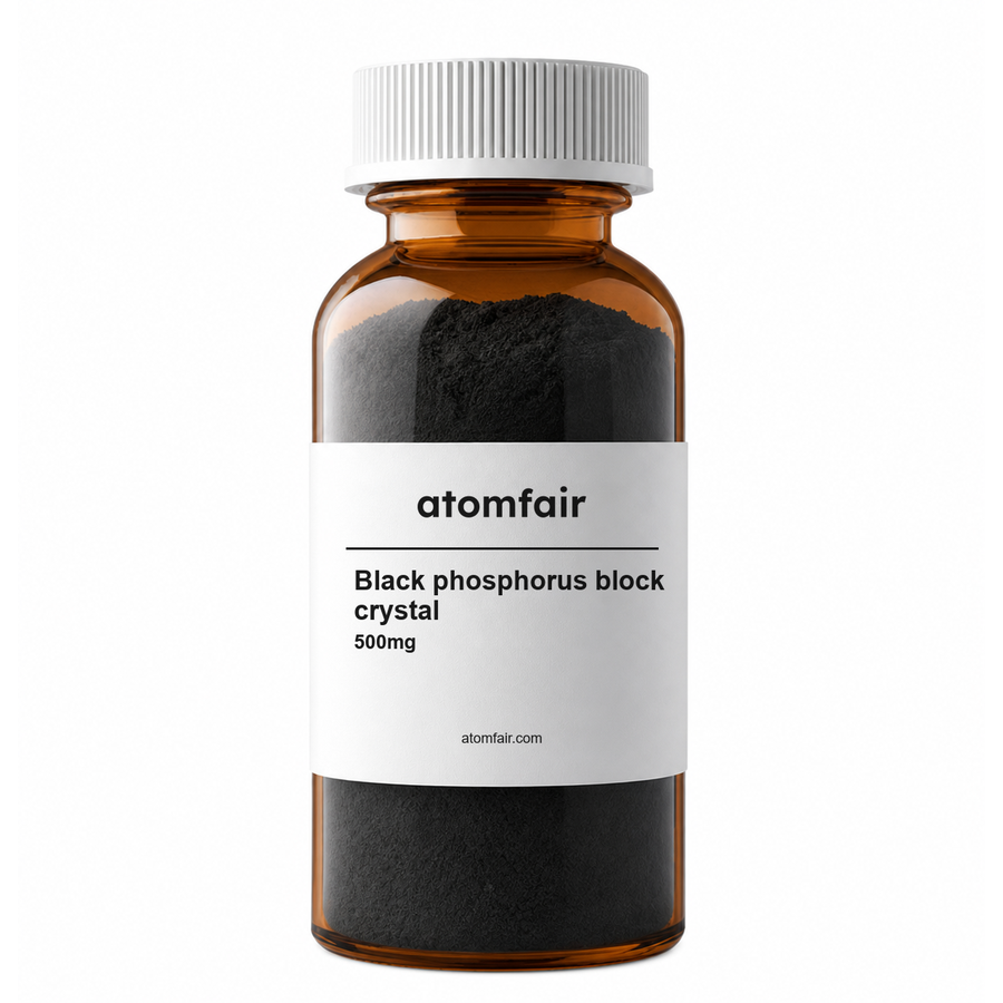
Black Phosphorus Block Crystal 500mg 1–10mm ATOMFAIR®
$222.00