
Silicon Wafers & Substrates
Silicon wafers and substrates are foundational materials for semiconductor device fabrication, MEMS, sensors, power electronics, photovoltaic research, thin-film deposition, and laboratory process development. This category covers silicon substrates in different wafer diameters, conductivity types, resistivity levels, crystal orientations, thicknesses, surface finishes, and oxide structures.
Whether you need a standard polished silicon wafer for laboratory experiments, a high-resistivity substrate for electrical or RF research, a double-side polished wafer for alignment and backside processing, or a thermally oxidized silicon wafer for dielectric and surface studies, the right selection should begin with the substrate material, wafer size, electrical properties, and surface requirements.
Use the selection guide below to compare the main silicon wafer formats and identify the specifications most relevant to your process equipment and application.
Show More: Silicon Wafers & Substrates
Product Structures
| Product Type | Main Characteristics | Typical Selection Direction |
|---|---|---|
| Monocrystalline silicon wafers | Uniform crystal structure and a stable, flat surface. | Device research, MEMS, sensors, thin-film deposition, and process development. |
| Single-side polished wafers (SSP) | One polished process surface, with a backside that may be etched or non-polished. | Front-side coating, lithography, processing, and surface characterization. |
| Double-side polished wafers (DSP) | Low-roughness polished surfaces on both sides. | Backside alignment, double-side lithography, optical inspection, bonding, and precision processing. |
| Thermally oxidized silicon wafers | A controlled silicon dioxide layer formed on the silicon surface. | Insulation, dielectric layers, masking, passivation, and surface studies. |
| SOI wafers | Device layer, buried insulating layer, and supporting silicon layer. | MEMS, microsensors, isolation structures, and advanced device research. |
| High-resistivity silicon wafers | Higher electrical resistivity to reduce substrate conduction. | RF, microwave, power devices, sensors, and electrical measurements. |
Conductivity Type and Resistivity
| Selection Factor | Common Options | Selection Considerations |
|---|---|---|
| N-Type silicon | Donor-doped silicon | Use when an N-type substrate or defined carrier behavior is required. |
| P-Type silicon | Acceptor-doped silicon | Use when a P-type substrate is required for device fabrication or comparison studies. |
| Low-resistivity silicon | Low-resistivity or heavily doped configurations | Useful when electrical conduction, backside contact, or current transport is important. |
| Medium-resistivity silicon | General-purpose resistivity ranges | Suitable for general device development, process validation, and material research. |
| High-resistivity silicon | High-resistivity, ultra-high-resistivity, or undoped configurations | Suitable for reducing parasitic conduction, RF loss, and electrical background effects. |
Resistivity should be selected together with the device structure, test frequency, contact design, doping requirements, and downstream process. For electrically sensitive applications, specifying only N-Type or P-Type may not be sufficient; the target resistivity range should also be defined.
Wafer Diameter
| Wafer Size | Typical Use Direction |
|---|---|
| 2 inch | Small-scale experiments, material screening, early process validation, and sample-level research. |
| 3 inch | Small-batch process development, MEMS, and sensor research. |
| 4 inch | Common laboratory lithography, deposition, etching, and device-development processes. |
| 6 inch | Larger-area process validation, process transfer, and multiple-device layouts. |
| 8 inch | Large-area process development, equipment compatibility studies, and improved usable area. |
Choose the diameter according to the available chuck, chamber, wafer carrier, mask, alignment system, and inspection equipment. A larger wafer is not automatically the better choice; equipment compatibility and usable process area are more important.
Surface Finish and Geometry
Important wafer specifications may include:
- Single-side or double-side polishing
- Surface roughness
- Nominal thickness and thickness tolerance
- Total thickness variation (TTV)
- Bow and warp
- Backside condition
- Edge profile and orientation notch
For general material research, diameter, thickness, and polishing are usually the first specifications to confirm. For lithography, bonding, deposition, and double-side processing, TTV, bow, warp, and backside roughness may also be critical.
Crystal Orientation
| Orientation | Selection Direction |
|---|---|
| <100> | Widely used for semiconductor processing, MEMS, lithography, and surface fabrication. |
| <111> | Used for specific etching behavior, surface structures, and crystallographic studies. |
| Custom orientation | Suitable when crystal-plane direction or etching behavior is process-specific. |
Crystal orientation can affect wet etching, surface atomic arrangement, thin-film growth, and device direction. If the process depends on a particular crystal plane, confirm the orientation and allowable deviation before ordering.
Thermal Oxide Silicon Wafers
Thermally oxidized silicon wafers combine a silicon substrate with a defined silicon dioxide layer. They can be selected according to oxide thickness, oxidation side, base wafer diameter, conductivity type, thickness, and surface finish.
| Parameter | Selection Direction |
|---|---|
| Oxidation side | Single-side or double-side oxidation. |
| Oxide thickness | Thin, medium, or application-specific customized thickness. |
| Base polish | SSP or DSP silicon substrate. |
| Base conductivity | N-Type, P-Type, high-resistivity, or another specified silicon base. |
| Functional use | Insulation, dielectric layers, masking, passivation, surface protection, or process comparison. |
How to Select a Silicon Wafer
- Confirm the wafer diameter supported by your equipment.
- Select N-Type, P-Type, high-resistivity, or undoped silicon according to the device and test requirements.
- Define the target resistivity range.
- Choose SSP or DSP according to the processing surfaces required.
- Select thickness based on equipment clamping, process depth, and mechanical strength.
- Confirm TTV, bow, and warp requirements for lithography, bonding, deposition, or double-side processing.
- Select a thermal oxide or SOI structure when insulation or an integrated dielectric layer is required.
- Confirm crystal orientation, edge profile, notch, cleanliness, and packaging requirements.
Typical Applications
- Semiconductor device research and process validation
- MEMS and microsensor fabrication
- Lithography, etching, deposition, and surface-treatment studies
- Thin-film growth and interface research
- RF, microwave, and electrical testing
- Power-device and isolation-structure research
- Thermal oxidation, dielectric-layer, and passivation experiments
- Optical, materials, and nanofabrication research
- Process development in university, institutional, and industrial laboratories
Frequently Asked Questions
Should I choose an N-Type or P-Type silicon wafer?
The choice depends on the device structure, doping design, contact configuration, and electrical testing requirements. If the process does not specify a conductivity type, review the process documentation or consult a technical specialist before ordering.
What is the difference between SSP and DSP?
SSP wafers are polished on one side and are generally suitable when processing is concentrated on the front surface. DSP wafers are polished on both sides and are preferred for backside alignment, double-side processing, optical inspection, bonding, or lower backside roughness.
What are high-resistivity silicon wafers used for?
High-resistivity wafers can reduce substrate conduction and parasitic electrical effects. They are commonly considered for RF, microwave, sensor, power-device, and electrically sensitive research.
How do I choose between 2-inch, 4-inch, and 6-inch wafers?
Start with the diameter supported by your equipment, wafer holder, mask, and process chamber. Smaller wafers are convenient for compact experiments, while larger wafers provide more usable area for process validation and multiple-device layouts.
Why is crystal orientation important?
Crystal orientation affects wet etching, crystal-plane structure, thin-film growth, and device direction. Common orientations such as <100> and <111> are not interchangeable for every process.
What is the difference between a thermal oxide wafer and a polished silicon wafer?
A polished silicon wafer provides a flat silicon surface for processing. A thermal oxide wafer adds a silicon dioxide layer that can be used for insulation, dielectric structures, masking, passivation, or surface protection.
Which specifications should I confirm besides diameter and thickness?
Confirm conductivity type, resistivity, crystal orientation, SSP or DSP finish, surface roughness, TTV, bow, warp, backside condition, edge profile, orientation notch, cleanliness, and packaging requirements.
Can silicon wafers be supplied with special specifications?
Special diameters, thicknesses, resistivity ranges, polishing requirements, crystal orientations, oxide thicknesses, and packaging configurations may be available upon request. When making an inquiry, provide the equipment limitations, intended application, quantity, and acceptable tolerances.
Showing all 15 results
-
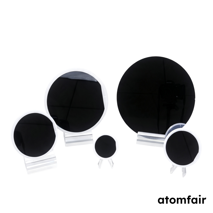
High-Resistivity 3 in SSP Silicon Wafer ATOMFAIR®
$32.90 -
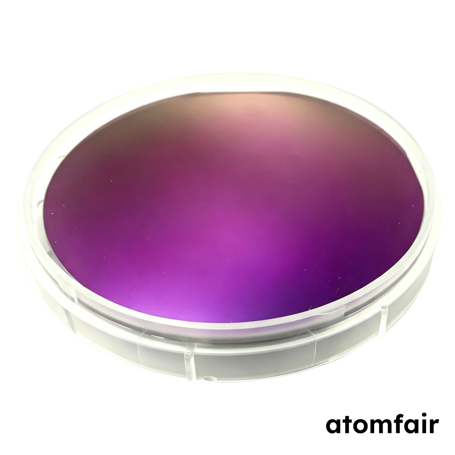
Monocrystalline Silicon Wafer 8 Inch 725±25μm ATOMFAIR®
$35.90 -
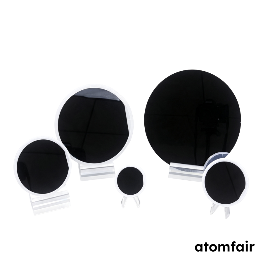
N-Type Silicon Wafer 2 in DSP 400μm ATOMFAIR®
$15.90 -
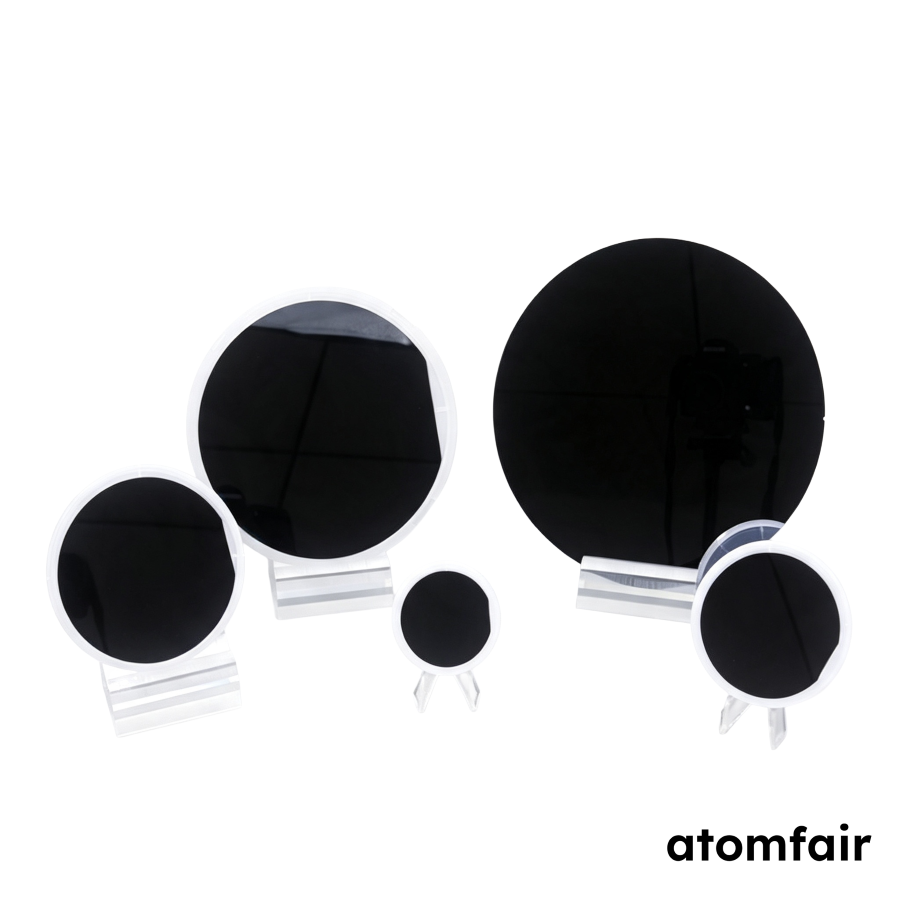
N-Type Silicon Wafer 2 in SSP 400 μm ATOMFAIR®
$19.90 -
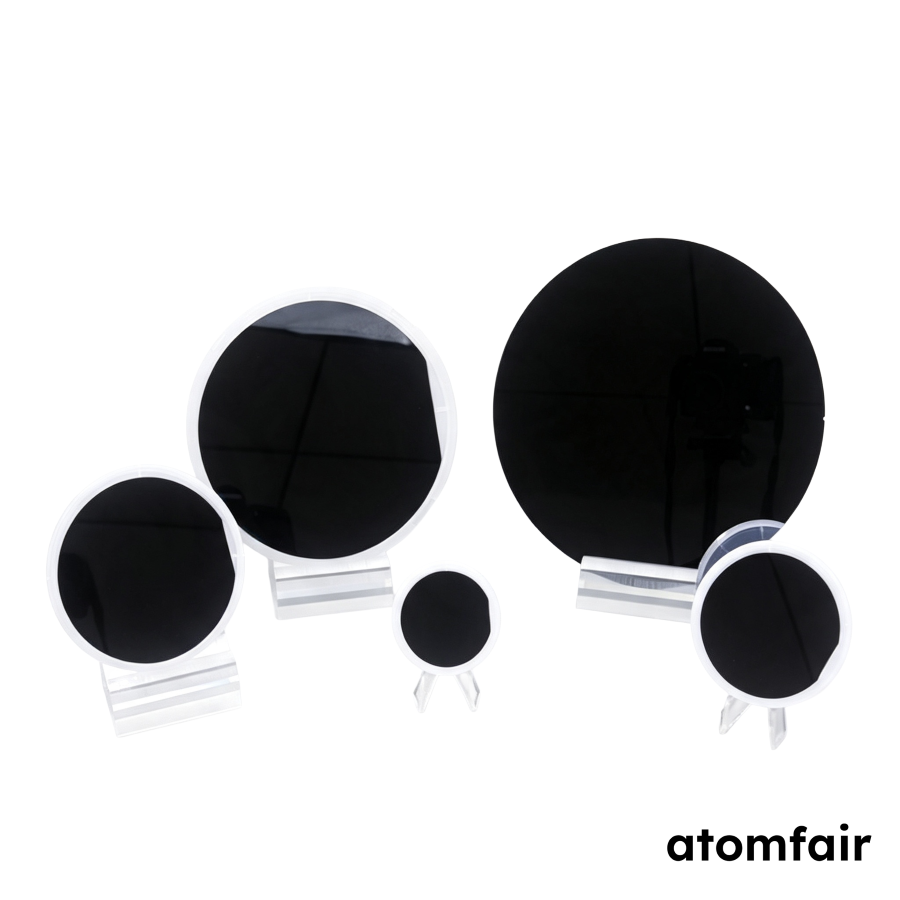
N-Type Silicon Wafer 2 inch 400μm SSP ATOMFAIR®
$15.90 -
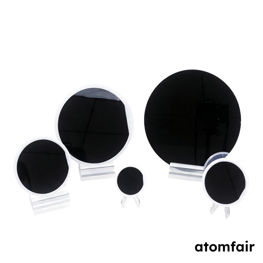
N-Type Silicon Wafer 4 in DSP 500μm ATOMFAIR®
$23.90 -
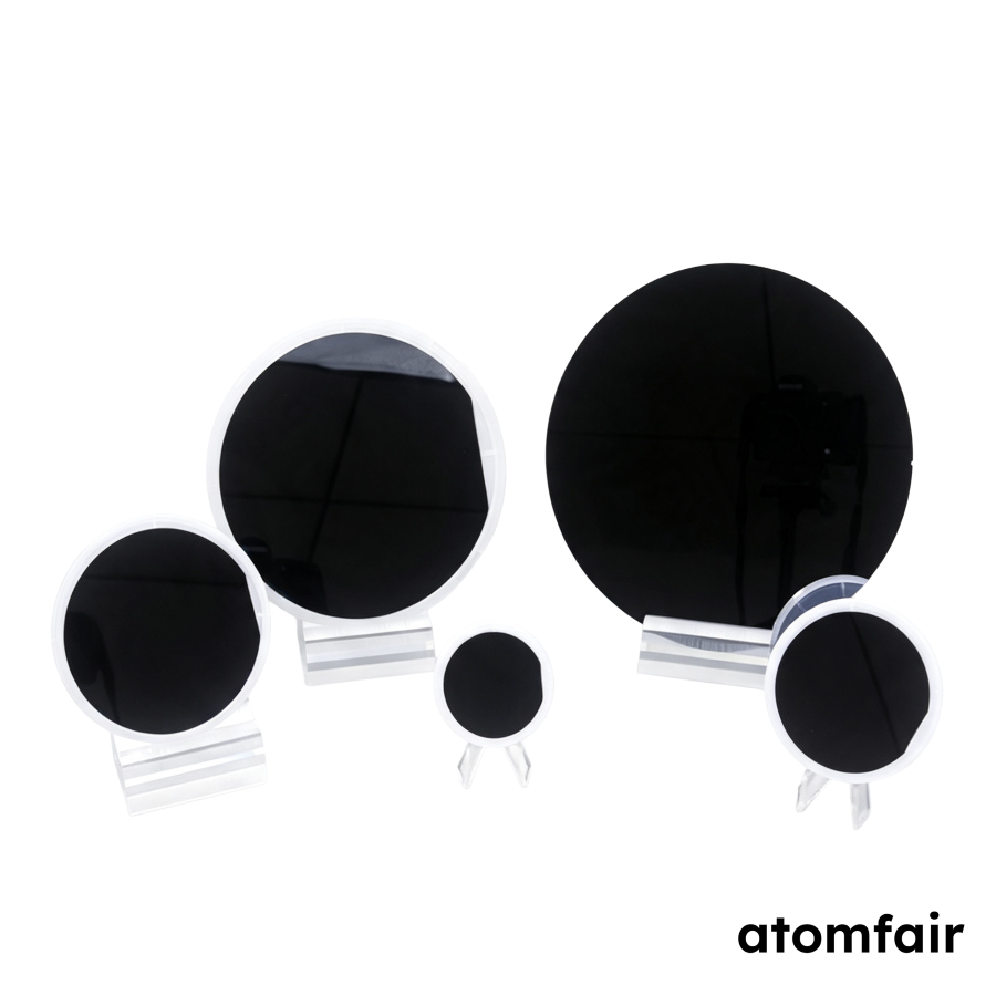
N-Type Silicon Wafer 6 in SSP 625μm ATOMFAIR®
$30.90 -
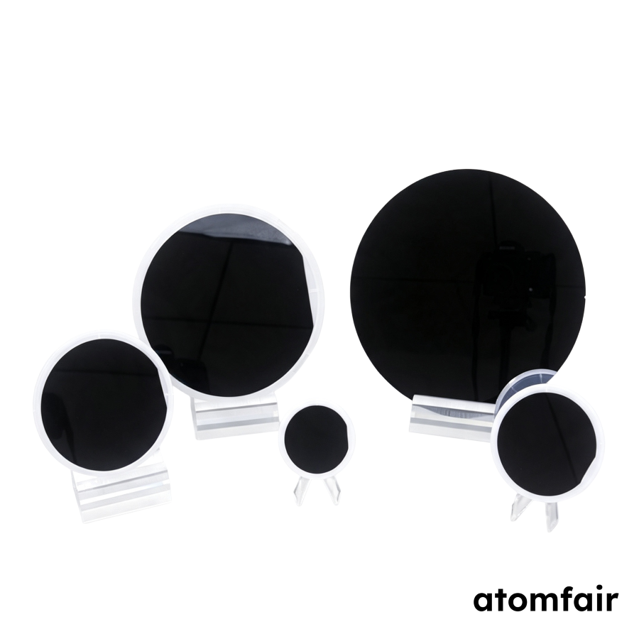
P-Type Silicon Wafer 150mm SSP 625μm ATOMFAIR®
$30.90 -
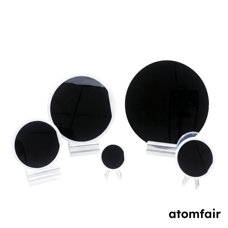
P-Type Silicon Wafer 2 Inch DSP 400μm ATOMFAIR®
$15.90 -
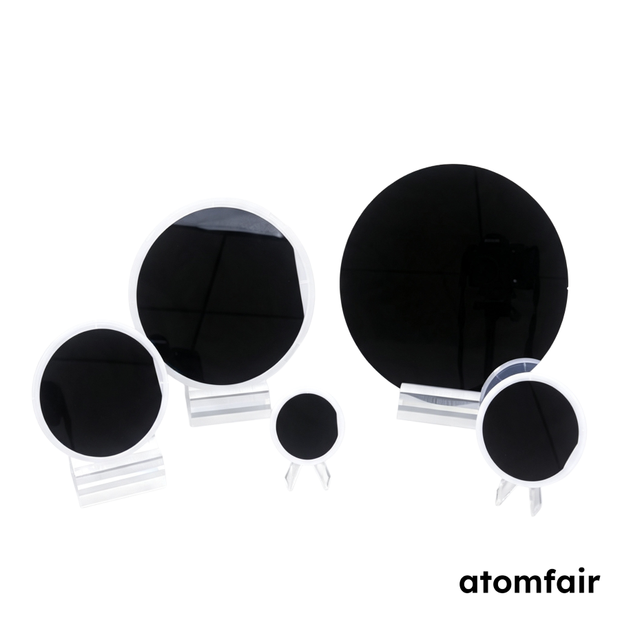
P-Type Silicon Wafer 2 inch SSP 400 μm ATOMFAIR®
$15.90 -
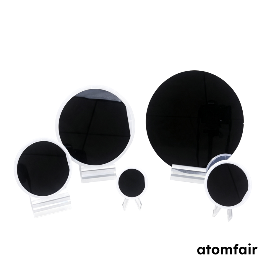
P-Type Silicon Wafer 4 in DSP 500 μm ATOMFAIR®
$23.90 -
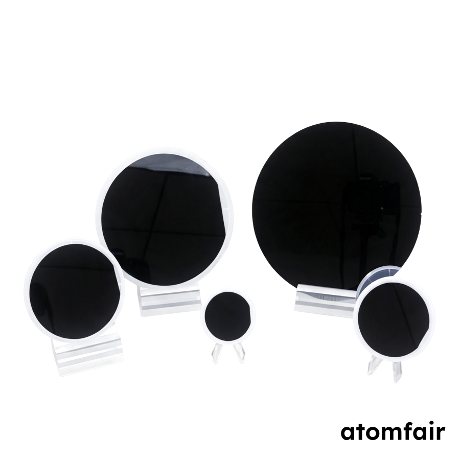
P-Type Silicon Wafer 4 inch SSP 500μm ATOMFAIR®
$23.90 -
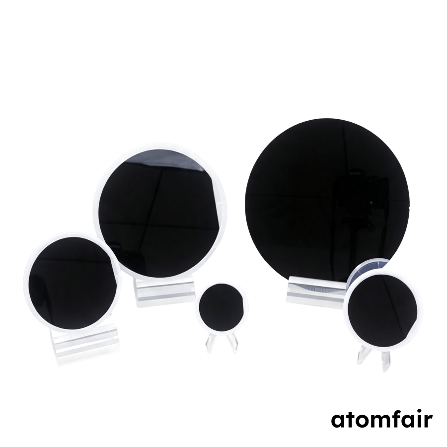
Silicon Wafer N-Type 4 in 500μm SSP ATOMFAIR®
$23.90 -
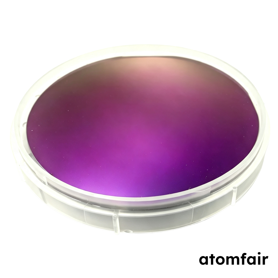
Thermal Oxidation Silicon Wafer 4 inch 285 nm ATOMFAIR®
$23.90 -
Thermal Oxide Silicon Wafer 2 in SSP 285 nm ATOMFAIR®
$17.90