|
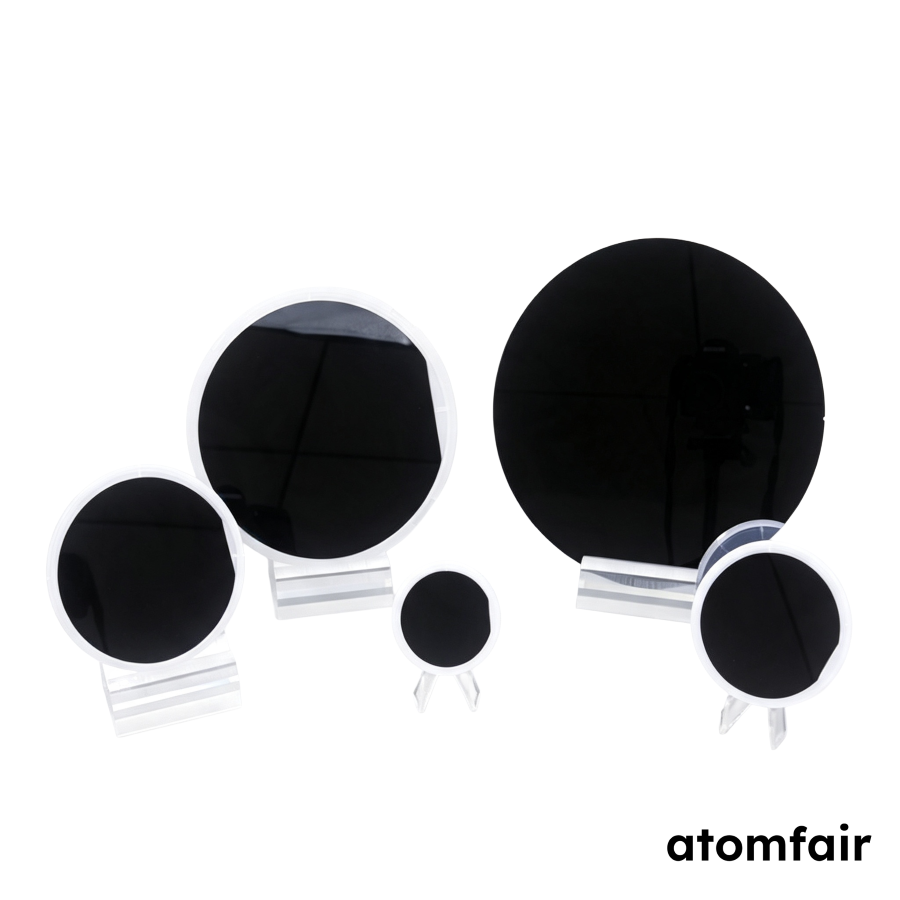
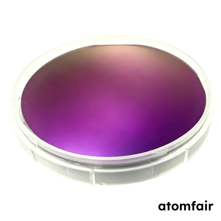
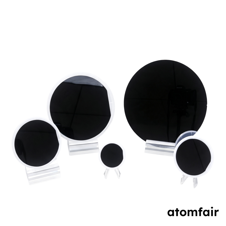
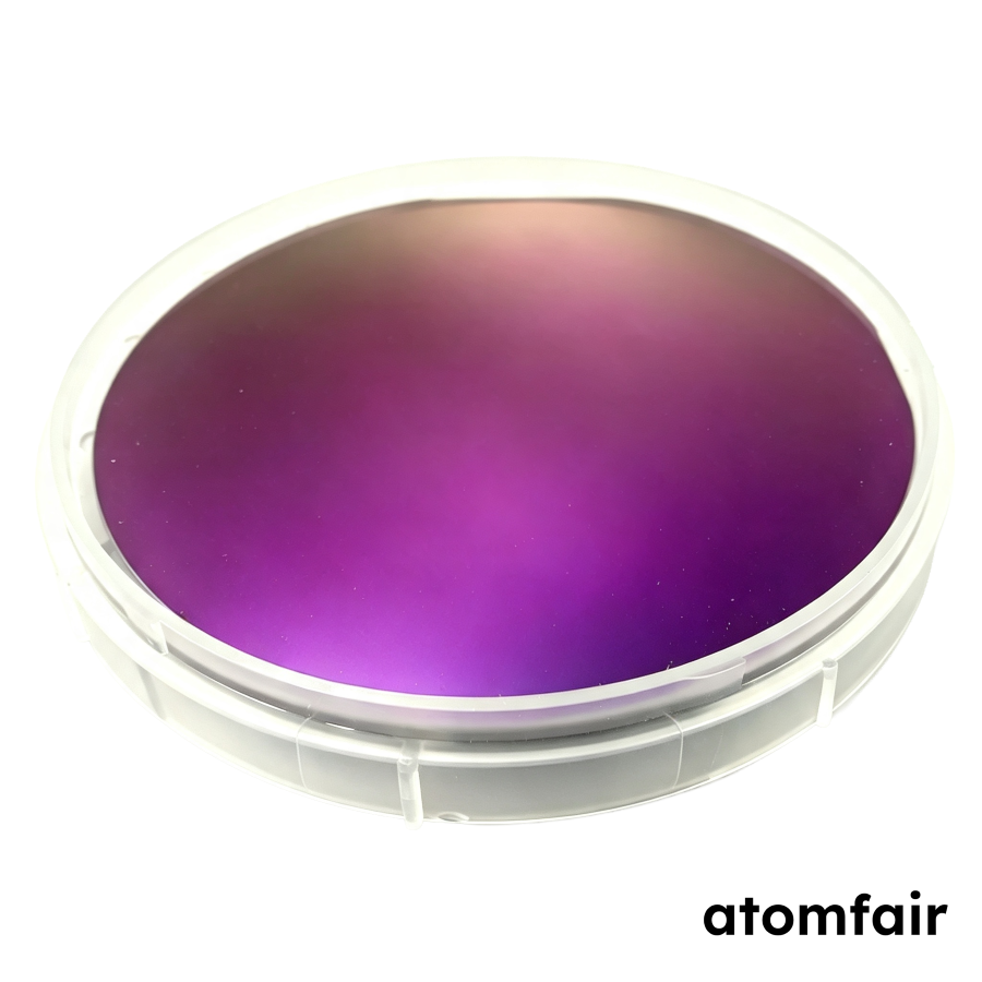
Thermal Oxidation Silicon Wafer – 4 inch (100 mm) Single-Side Polished, Double-sided oxidation 285 nm
Product Type: Thermal oxidation silicon wafer
Research-grade laboratory product
|
|||||||||||||||||||||||
|
|||||||||||||||||||||||
|
PRODUCT SELECTION SUPPORT
For model selection, material matching or specification support, contact our technical sales team.
E-MAIL: inquiry@atomfair.com
|
|||||||||||||||||||||||
|
Manufacturer: Atomfair LLC
Brand: ATOMFAIR®
|
Environmental contamination and mechanical damage must be minimized to preserve oxide layer integrity. Moisture and particulate exposure can compromise surface quality and oxide uniformity.
- Contamination Control: Store wafers in cleanroom-compatible containers at controlled temperature and humidity to prevent particulate adhesion and moisture-induced oxide degradation.
- Mechanical Handling: Handle wafers only with clean, non-marring tweezers or vacuum wands to avoid scratches or chipping on the polished single-side surface.
- Oxide Layer Sensitivity: Avoid excessive thermal shock or rapid temperature changes, as differential expansion can induce stress cracks in the 285 nm oxide layer.
Use this sequence to safely unpack, inspect, and store a 4-inch double-side oxidized wafer prior to processing. Proper initial handling prevents contamination and mechanical damage to the oxide layer and polished surface.
Required Equipment: Cleanroom gloves (nitrile or latex), PTFE-coated wafer tweezers
- Inspect packaging integrity
Inspect the outer packaging for breaches or moisture indicators before transferring the wafer to a cleanroom environment. - Don cleanroom gloves
Don cleanroom gloves and use PTFE-coated wafer tweezers to extract the wafer from its cassette or container. - Visually examine the wafer
Visually examine the wafer under a bright light for chips, cracks, or visible contamination on both the polished and oxide surfaces. - Place the wafer into a clean storage box
Place the wafer into a cleanroom-grade storage box with the polished side facing upward and secure the lid. - Record storage conditions
Record the storage temperature and humidity levels if the wafer will remain outside a vacuum enclosure for more than 24 hours.
What is the thickness tolerance of the base silicon wafer for the Atomfair AF-OXI-4SSP285 thermal oxidation wafer?
The base wafer thickness is specified as 500 +/- 25 um, providing a tolerance of ±25 microns for the 4 inch (100 mm) diameter substrate.
What oxide thickness options are available for the double-sided thermal oxidation on this 4 inch wafer?
The standard oxide thickness is 285 nm, with a customizable range of 20 to 2000 nm available upon request for specific research requirements.
What is the base material specification for the Atomfair thermal oxidation silicon wafer?
The base wafer is made from 6N monocrystalline silicon, available in either CZ (Czochralski) or FZ (Float Zone) growth methods, as per the product specification.
4-inch thermal oxidation silicon wafer with double-sided 285 nm oxide layer on single-side polished monocrystalline silicon substrate, offering a customizable oxide thickness range of 20-2000 nm for research and device fabrication.
Positive
- Double-sided oxide layer: Provides uniform thermal oxide on both wafer surfaces, enabling symmetric dielectric isolation for devices such as MEMS or capacitive sensors.
- Customizable oxide thickness range: Oxide thickness can be specified from 20 to 2000 nm, allowing precise tuning of electrical and optical properties for specific process requirements.
Trade-offs
- Single-side polished finish: Only one side is polished; the unpolished backside may introduce surface roughness that complicates processes requiring double-side smoothness or adhesion.
- Base thickness tolerance ±25 µm: The 500 µm nominal thickness with ±25 µm tolerance demands careful process integration for applications sensitive to wafer thickness uniformity.
Every advanced material, component, equipment, and instrument in our catalog is backed by rigorous testing. We maintain strict internal quality management frameworks and align with CE conformity metrics to deliver transparent, reproducible performance data via our public open-science repository.
To request raw batch performance data, submit formal vendor registration paperwork, or execute a fast-turnaround R&D manufacturing loop, contact us at inquiry@atomfair.com.
Item is dispatched under the Atomfair Shipping & Delivery Framework (Free worldwide shipping on orders over $59 USD excl. heavy equipment). Return is governed by the Atomfair Return & Refund Policy (7-day technical return window).