|
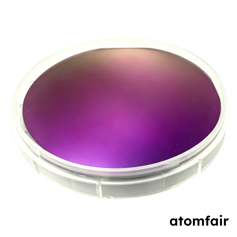
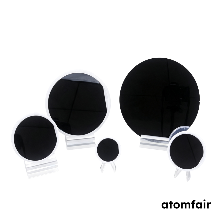
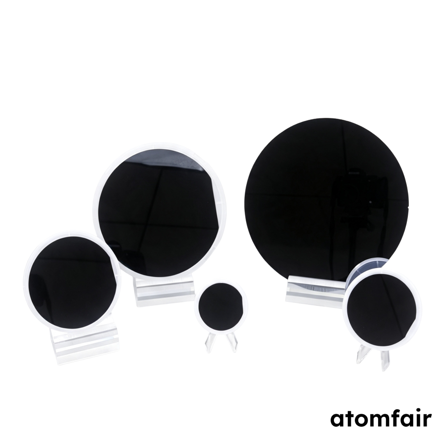
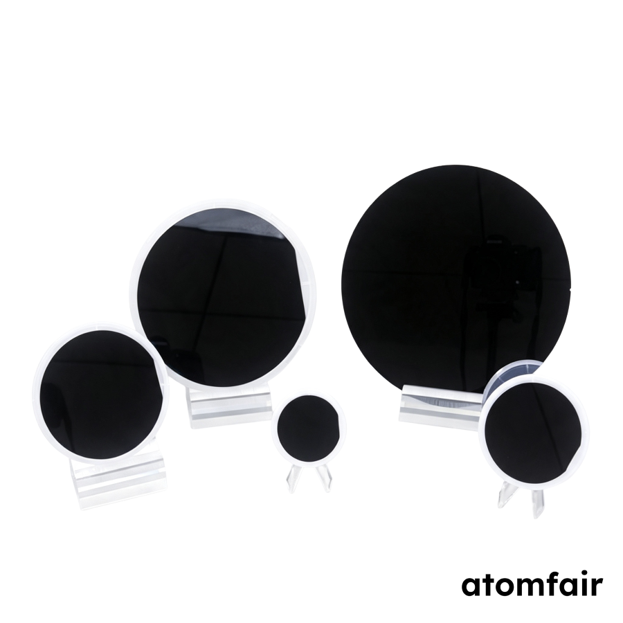
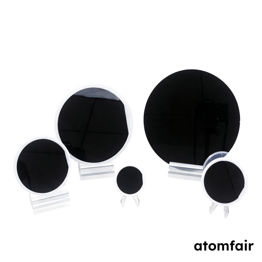
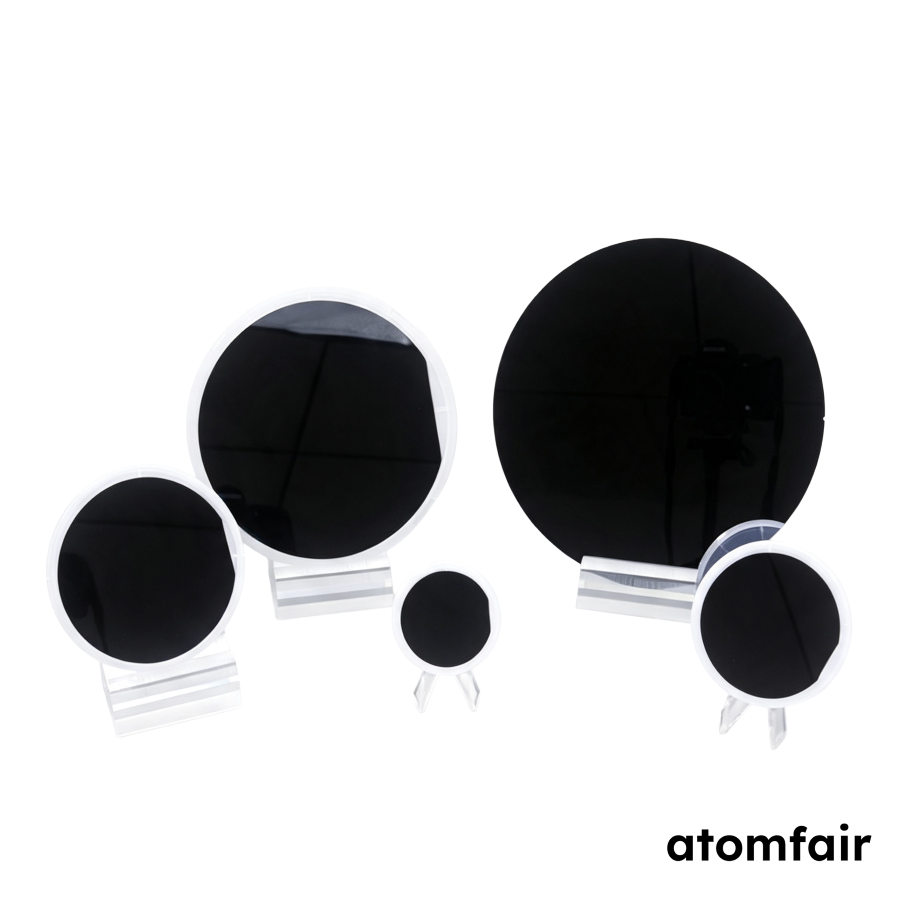
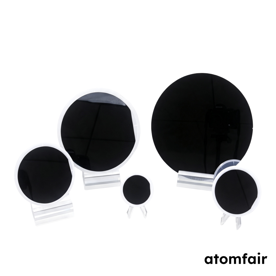
High resistivity undoped Monocrystalline Silicon Wafer – 3 inch (76.2 mm) <100> Single-Side Polished
Product Type: Silicon wafer
Research-grade laboratory product
|
|||||||||||||||||||||||||||||||||||
|
|||||||||||||||||||||||||||||||||||
|
PRODUCT SELECTION SUPPORT
For model selection, material matching or specification support, contact our technical sales team.
E-MAIL: inquiry@atomfair.com
|
|||||||||||||||||||||||||||||||||||
|
Manufacturer: Atomfair LLC
Brand: ATOMFAIR®
|
What is the significance of >10K ohm.cm resistivity in undoped silicon wafers for RF and photonic applications?
The >10K ohm.cm resistivity indicates minimal free carrier concentration, which reduces RF losses and optical absorption in the near-infrared. This is achieved using undoped 6N CZ/FZ monocrystalline silicon, suitable for high-Q resonators, THz optics, and radiation detectors requiring low leakage current.
How do the wafer geometry tolerances (TTV, BOW, WARP) affect compatibility with mask alignment and thin-film deposition tools?
With TTV <10 um, BOW <10 um, and WARP <15 um, this wafer ensures uniform photoresist coating and reliable mask alignment across the 3-inch diameter. The thickness tolerance of 400 +/- 25 um also maintains consistent plasma etch uniformity. These tolerances are critical for multi-layer lithography processes.
Why is the back side of this wafer etched rather than polished, and what are the implications for handling and processing?
The back side is etched to provide a matte finish that reduces particle generation and minimizes stress-induced warpage during thermal cycling. The etched back side also avoids backside reflections during photolithography, simplifying alignment. The front side maintains Ra <0.5 nm for high-resolution patterning.
This 3-inch high-resistivity undoped monocrystalline silicon wafer with <100> orientation and single-side polished finish offers tight geometry tolerances (TTV<10 µm, BOW<10 µm, WARP<15 µm) and low front-side roughness (Ra<0.5 nm), making it suitable for research-grade device fabrication requiring high resistivity substrates.
Positive
- High resistivity undoped silicon: Resistivity >10K ohm.cm enables intrinsic electrical behavior, critical for high-frequency or high-voltage device research without doping artifacts.
- Tight geometric tolerances: TTV <10 µm, BOW <10 µm, and WARP <15 µm ensure uniform thickness and flatness, reducing processing variability during lithography and thin-film deposition.
Trade-offs
- Thin wafer handling risk: At 400 ±25 µm thickness, the wafer is relatively fragile and requires careful handling during manual transfer or processing to avoid breakage.
- Single-side polished only: Back side is etched (not polished), limiting use to applications requiring only one smooth surface; double-sided polishing is not available per this configuration.
Every advanced material, component, equipment, and instrument in our catalog is backed by rigorous testing. We maintain strict internal quality management frameworks and align with CE conformity metrics to deliver transparent, reproducible performance data via our public open-science repository.
To request raw batch performance data, submit formal vendor registration paperwork, or execute a fast-turnaround R&D manufacturing loop, contact us at inquiry@atomfair.com.
Item is dispatched under the Atomfair Shipping & Delivery Framework (Free worldwide shipping on orders over $59 USD excl. heavy equipment). Return is governed by the Atomfair Return & Refund Policy (7-day technical return window).