|
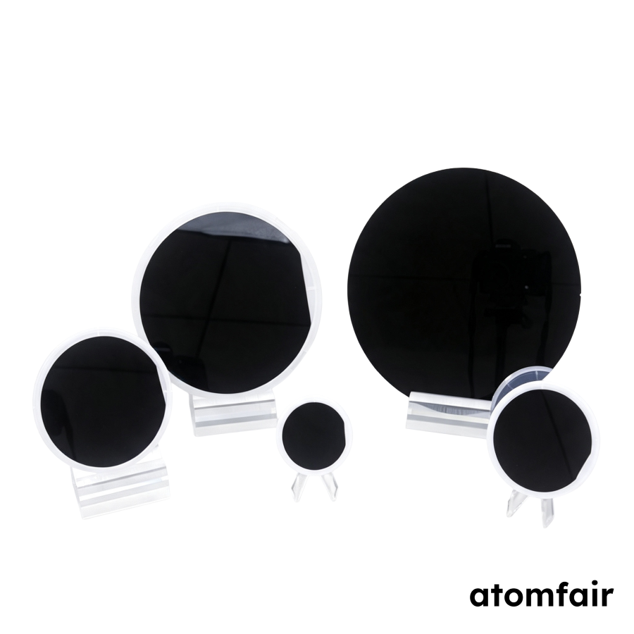
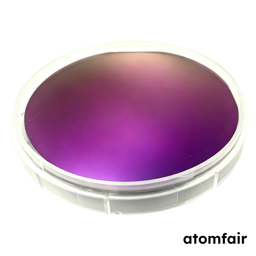
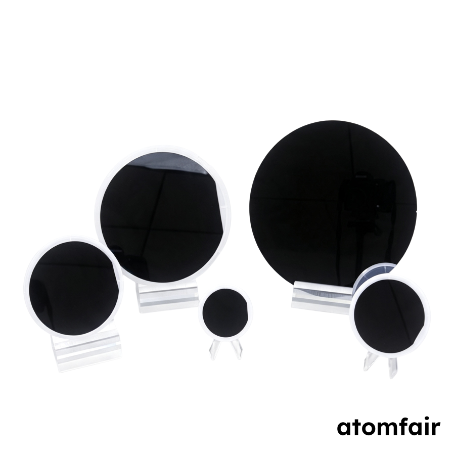
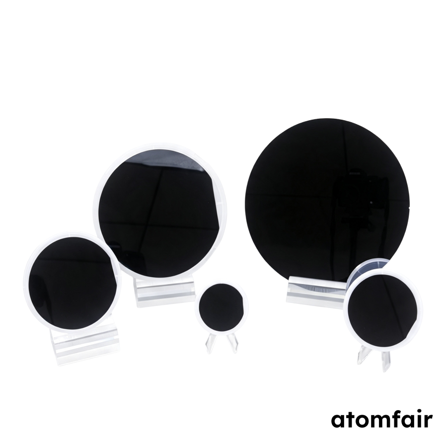
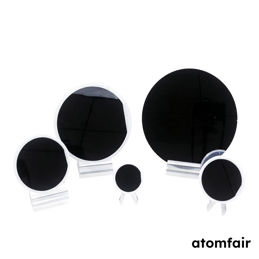
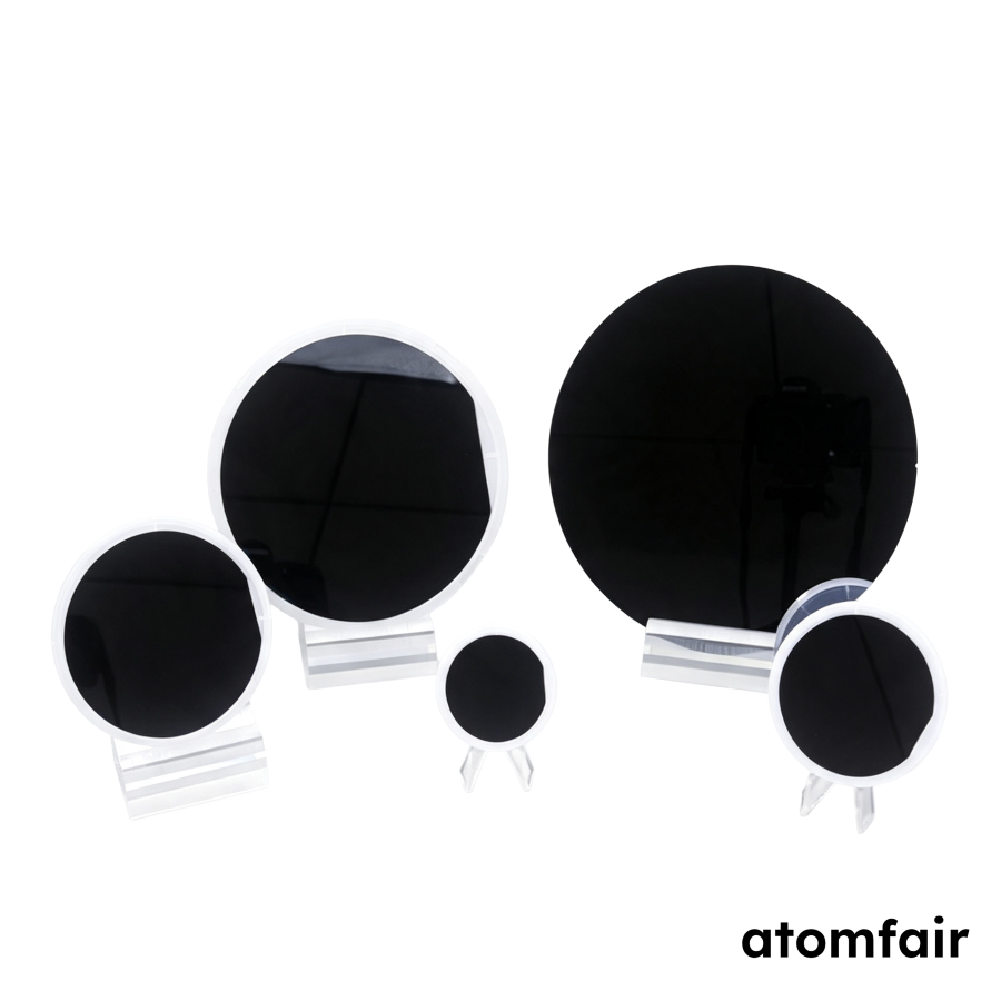
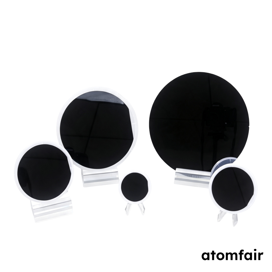
N type Monocrystalline Silicon Wafer – 2 inch (50.8 mm) <100> Single-Side Polished
Product Type: Silicon wafer
Research-grade laboratory product
|
|||||||||||||||||||||||||||||||||||
|
|||||||||||||||||||||||||||||||||||
|
PRODUCT SELECTION SUPPORT
For model selection, material matching or specification support, contact our technical sales team.
E-MAIL: inquiry@atomfair.com
|
|||||||||||||||||||||||||||||||||||
|
Manufacturer: Atomfair LLC
Brand: ATOMFAIR®
|
How does the resistivity selection for the 2-inch N-type <100> silicon wafer influence its suitability for power electronics versus high-resistivity RF applications?
The wafer offers selectable resistivity values ranging from 0.001-0.005 ohm.cm (low resistivity for high-current power devices) to >10K ohm.cm (high resistivity for RF/analog applications requiring low parasitic capacitance). The N-type phosphorus doping provides consistent carrier concentration across the entire 6N-grade monocrystalline silicon CZ or FZ material, enabling tailoring of the wafer to the specific device operating voltage and frequency regime.
Is the back side of the single-side polished 2-inch N-type silicon wafer suitable for direct bonding or subsequent epitaxial growth without additional surface preparation?
No, the back side is etched (not polished) with a surface roughness higher than the front side's Ra <0.5 nm. For direct bonding, epitaxial deposition, or other processes requiring a smooth, defect-free surface, additional polishing or planarization of the back side would be necessary. The single-side polished configuration is designed for applications where only the front side requires high-quality surface finish.
What are the critical flatness parameters of the 2-inch N-type <100> silicon wafer and how do they affect photolithography alignment and thin-film uniformity?
The wafer exhibits TTV <5 um, BOW <10 um, and WARP <10 um, ensuring tight focal plane control and minimal stress-induced distortion during photolithography. These flatness specifications are critical for maintaining sub-micron alignment accuracy across the 50.8 mm diameter and for achieving uniform film thickness in sputtering, evaporation, or CVD processes.
This 2-inch N-type <100> monocrystalline silicon wafer offers 6N purity with CZ/FZ material options, tight geometric tolerances (TTV <5 µm, BOW/WARP <10 µm, Ra <0.5 nm), and selectable resistivity ranges, making it suitable for research-grade semiconductor and photonics applications. The single-side polished finish with etched backside should be considered for process compatibility.
Positive
- High-purity 6N monocrystalline silicon: Available in CZ or FZ growth methods, providing low defect density and consistent electronic properties for advanced device fabrication and research.
- Tight geometric tolerances: TTV <5 µm, BOW <10 µm, WARP <10 µm, and front-side roughness Ra <0.5 nm ensure uniform processing and reproducible results in lithography, epitaxy, and thin-film deposition.
Trade-offs
- Single-side polished only: Back side is etched; applications requiring double-side polished wafers or specific backside treatments will need alternate configurations.
- Thickness tolerance ±25 µm: The 400 ±25 µm thickness range may be a constraint for processes demanding extremely tight thickness uniformity, such as certain MEMS or high-frequency device stacks.
Every advanced material, component, equipment, and instrument in our catalog is backed by rigorous testing. We maintain strict internal quality management frameworks and align with CE conformity metrics to deliver transparent, reproducible performance data via our public open-science repository.
To request raw batch performance data, submit formal vendor registration paperwork, or execute a fast-turnaround R&D manufacturing loop, contact us at inquiry@atomfair.com.
Item is dispatched under the Atomfair Shipping & Delivery Framework (Free worldwide shipping on orders over $59 USD excl. heavy equipment). Return is governed by the Atomfair Return & Refund Policy (7-day technical return window).