
Deposition, Etching & Process Materials
Deposition, Etching & Process Materials are used to build, modify, pattern, and clean semiconductor and functional thin-film structures. This category covers materials for sputtering, evaporation, CVD, PECVD, ALD, wet etching, dry etching, plasma processing, wafer cleaning, surface treatment, and related process steps.
Products can be selected by process method, material system, physical form, purity, substrate compatibility, and required film or etching performance. Whether you are preparing a conductive layer, dielectric film, diffusion barrier, compound-semiconductor structure, micro-pattern, or clean process surface, the material should be matched to the equipment, substrate, film stack, and process conditions.
Use the selection guidance below to compare deposition sources, precursors, etching materials, process gases, cleaning chemicals, and surface-treatment products according to their intended process function and specification requirements.
Show More: Deposition, Etching & Process Materials
Deposition Materials
| Product Family | Common Forms | Typical Uses | Main Selection Points |
|---|---|---|---|
| Sputtering targets | Round targets, rectangular targets, bonded targets | Metal films, dielectric films, transparent conductive films, barrier layers | Composition, purity, dimensions, thickness, density, bonding, backing plate |
| Evaporation materials | Pellets, granules, wires, pieces, tablets | Electrodes, contacts, reflective films, optical coatings | Material, purity, melting point, evaporation behavior, crucible compatibility |
| CVD precursors | Liquid, solid, gas, ampoule, or bubbler delivery | Silicon, oxide, nitride, carbide, and metal films | Deposition temperature, vapor pressure, delivery method, carrier gas, film chemistry |
| ALD precursors | Liquid or solid precursor systems | High-aspect-ratio structures, dielectric layers, barrier layers, functional films | Thermal window, pulse behavior, surface reaction, purge requirements |
| PECVD process materials | Film precursors and reactive gas systems | Low-temperature dielectric, passivation, and protective coatings | Plasma compatibility, substrate temperature, film stress, residue control |
| Compound and functional materials | Oxides, nitrides, carbides, sulfides, selenides, alloys, composites | Optoelectronic, magnetic, sensor, RF, and power-device research | Stoichiometry, purity, phase, substrate, atmosphere, source format |
Selecting Materials by Film Function
| Target Film or Function | Material Systems to Compare | Specifications to Confirm |
|---|---|---|
| Conductive electrodes and interconnects | Aluminum, copper, gold, silver, platinum, titanium, chromium, nickel, multilayer metal systems | Conductivity, adhesion, thickness, roughness, oxidation resistance |
| Adhesion and diffusion-barrier layers | Titanium, chromium, tantalum, tungsten, molybdenum, related compounds | Adhesion, diffusion resistance, thermal stability, adjacent-layer compatibility |
| Dielectric and insulating films | Silicon dioxide, silicon nitride, aluminum oxide, hafnium oxide, other dielectric systems | Dielectric performance, breakdown behavior, film stress, thickness, uniformity |
| Transparent conductive films | ITO and other transparent conductive oxides | Optical transmission, sheet resistance, composition, substrate temperature |
| Optical and reflective films | Aluminum, silver, gold, dielectric stacks, specialty compounds | Reflectance, wavelength range, surface quality, adhesion |
| High-temperature functional films | Refractory metals, carbides, nitrides, ceramic compounds | Thermal stability, chemical resistance, stress, process atmosphere |
| Compound-semiconductor films | III-V materials, wide-bandgap materials, related source systems | Stoichiometry, lattice compatibility, substrate, temperature, layer structure |
Etching Materials
Etching materials should be selected according to the film being removed, the structures that must remain, the required selectivity, the etch rate, and the final surface profile.
| Etching Material Family | Typical Applications | Selection Considerations |
|---|---|---|
| Silicon etchants | Wafer thinning, trenches, cavities, MEMS structures, surface patterning | Crystal orientation, anisotropy, etch rate, temperature, surface finish |
| Oxide etchants | Silicon dioxide removal, pattern transfer, surface preparation | Selectivity, concentration, undercut, residue, metal compatibility |
| Nitride and ceramic etchants | Silicon nitride, metal nitride, ceramic and hard-mask processing | Selectivity to oxide, silicon, metal, and photoresist; process temperature |
| Metal etchants | Aluminum, copper, titanium, chromium, nickel, gold, multilayer metal films | Etch rate, corrosion, undercut, surface condition, waste handling |
| Compound-semiconductor etchants | GaAs, InP, GaN, SiC, and related semiconductor materials | Selectivity, crystal-plane effects, surface damage, residue, uniformity |
| Buffered and selective etchants | Controlled removal of selected films in multilayer structures | Stable etch rate, selectivity, repeatability, adjacent-layer compatibility |
| Dry-etch and plasma materials | Reactive-ion etching, plasma etching, high-aspect-ratio pattern transfer | Gas composition, anisotropy, sidewall profile, selectivity, residue control |
Process Gases, Cleaning and Surface-Treatment Materials
| Product Family | Main Function | Selection Focus |
|---|---|---|
| Reactive process gases | Deposition, oxidation, nitridation, etching, and plasma reactions | Gas purity, mixture ratio, flow range, cylinder or canister format |
| Plasma process gases | Anisotropic etching, cleaning, activation, and surface modification | Gas system, pressure, power, reaction by-products |
| Oxidation and nitridation materials | Formation of oxide, nitride, or composite dielectric layers | Film composition, temperature, thickness control, substrate compatibility |
| Wafer-cleaning chemicals | Removal of particles, organic residues, metallic contamination, and process by-products | Cleaning strength, material compatibility, residue, concentration, temperature |
| Surface-activation materials | Improvement of wettability, adhesion, bonding, or subsequent film growth | Surface energy, treatment time, post-treatment stability |
| Strippers and residue removers | Removal of photoresist, polymers, and etching residues | Selectivity, corrosion, swelling, temperature, rinsing requirements |
| Passivation and protective materials | Surface protection during storage, transfer, or subsequent processing | Film compatibility, removal method, cleanliness, thermal stability |
How to Choose the Right Process Material
| Main Requirement | Product Directions to Compare | Confirm Before Purchase |
|---|---|---|
| Uniform thin-film deposition | Sputtering targets, evaporation materials, CVD or ALD precursors | Film composition, thickness, uniformity, purity, equipment interface |
| Conformal coating on complex structures | ALD or CVD precursor systems | Feature aspect ratio, deposition temperature, delivery method, conformality |
| Low-temperature deposition | PECVD materials, plasma materials, low-temperature precursors | Substrate temperature, plasma conditions, film stress, residues |
| Fine pattern transfer | Dry-etch materials or selective wet etchants | Sidewall profile, selectivity, anisotropy, residue control |
| Fast removal of thicker films | Wet etchants or high-rate plasma processes | Etch rate, surface roughness, temperature, chemical compatibility |
| Reduced substrate damage | Low-energy plasma or mild selective etching systems | Ion energy, charging, surface damage, post-process cleaning |
| High-purity processing | High-purity targets, precursors, gases, and chemicals | Impurity limits, particles, moisture, packaging, documentation |
| Multilayer film processing | Compatible deposition and etching material combinations | Layer interaction, adhesion, selectivity, thermal sequence |
| Optical and transparent structures | Transparent conductive films, dielectric films, optical coatings | Wavelength, transmission, reflectance, roughness, film stress |
| High-temperature or corrosive processing | Refractory metals, ceramics, corrosion-resistant precursors and process materials | Operating temperature, atmosphere, corrosion, volatility, outgassing |
Specifications to Compare
Depending on the product type, the following specifications may be important:
- Material name, chemical composition, and stoichiometry
- Purity and impurity limits
- Physical form of the target, source, precursor, gas, or chemical
- Dimensions, thickness, density, and backing requirements
- Precursor state, vapor pressure, and delivery method
- Etch rate, selectivity, and etch uniformity
- Film thickness, uniformity, roughness, and film stress
- Deposition or etching temperature
- Process gas composition and purity
- Compatibility with the substrate and multilayer film structure
- Storage conditions, moisture sensitivity, and packaging
- Quantity, container format, and safety documentation
For a quotation, provide the intended process, equipment type, material system, substrate, dimensions, purity, quantity, and most important performance requirements. This information helps identify a suitable product specification.
Typical Applications
- Semiconductor device fabrication and process development
- MEMS and microsensor processing
- Thin-film transistor and display research
- Compound-semiconductor and wide-bandgap device development
- RF, microwave, and power-electronics research
- Photonic, optical, and optoelectronic thin films
- Metal electrodes and interconnects
- Dielectric, barrier, and passivation layers
- Wafer cleaning and surface preparation
- Plasma etching and micro-pattern transfer
- High-aspect-ratio structures and multilayer film processing
- University, institutional, and industrial process laboratories
Frequently Asked Questions
How do I choose between a sputtering target and an evaporation material?
Choose according to your deposition equipment. Sputtering systems usually require a target with compatible dimensions, thickness, density, backing, and bonding configuration. Evaporation systems commonly use pellets, granules, wires, pieces, or tablets selected for the crucible and evaporation source.
What information should I provide when buying a deposition material?
Provide the material composition, purity, deposition method, target or source dimensions, substrate type, wafer size, quantity, and any requirements for conductivity, transparency, dielectric performance, or optical behavior.
How do I choose an etching material?
First identify the film to be removed and the layers that must remain. Then compare etch rate, selectivity, undercut, surface damage, residue, temperature, and compatibility with the complete film stack.
What is the difference between wet etching and dry etching?
Wet etching uses a liquid chemical and is often selected for solution-based processing or bulk material removal. Dry etching uses reactive gases or plasma and is commonly chosen for fine patterns, directional profiles, and high-aspect-ratio structures.
Which materials are commonly used for dielectric films?
Common choices include silicon dioxide, silicon nitride, aluminum oxide, hafnium oxide, and other oxide, nitride, and multilayer dielectric systems. The appropriate choice depends on dielectric performance, film thickness, stress, process temperature, and device structure.
What should I consider when selecting a CVD or ALD precursor?
Consider the target film composition, deposition temperature, precursor state, vapor pressure, reaction activity, carrier gas, pulse and purge requirements, and compatibility with the reactor, substrate, and other layers.
Is higher purity always better?
Not necessarily. Purity should match the device performance, contamination-control requirements, and process budget. In addition to purity, particles, moisture, stoichiometry, physical form, packaging, and equipment compatibility should also be considered.
Can the same material be used for different deposition processes?
Not always. A material suitable for sputtering may not have the form, purity, vapor-pressure behavior, or delivery characteristics required for evaporation, CVD, or ALD. Confirm the process method, equipment interface, and material form before ordering.
Can deposition and etching materials be supplied to custom specifications?
Custom dimensions, compositions, purity levels, bonded targets, precursor packaging, gas mixtures, and process-specific chemical formulations may be available. Provide the equipment conditions, film stack, quantity, and technical requirements for evaluation.
What safety information should I review?
Before use, review the SDS, concentration or gas composition, storage conditions, container compatibility, ventilation, exhaust, abatement, transport requirements, and waste-disposal procedures. Materials should be handled according to applicable laboratory and process-safety requirements.
Showing 17–26 of 26 results
-
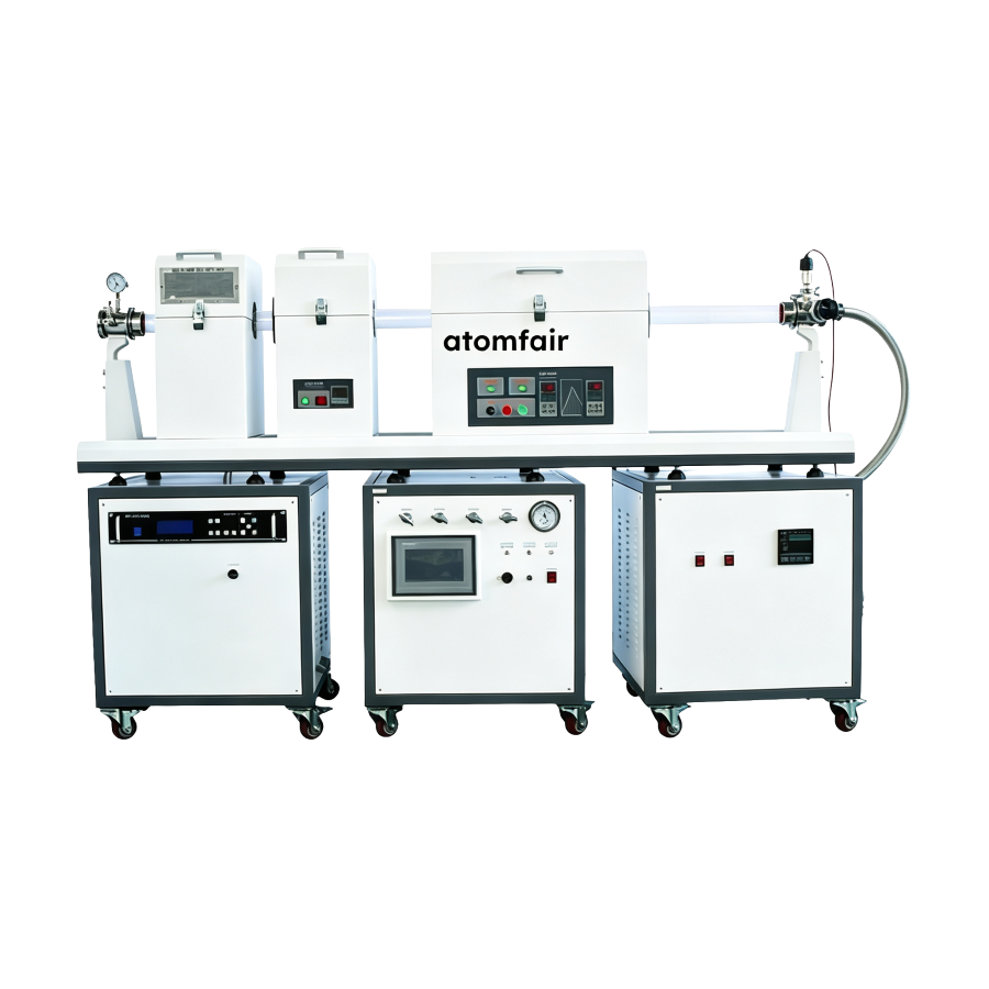
Rotating Intelligent PECVD System 1200 °C 500 W RF ATOMFAIR®
$23,500.00 -
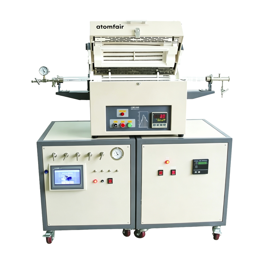
Single-Zone High-Temperature CVD System 1700 °C ATOMFAIR®
$21,500.00 -
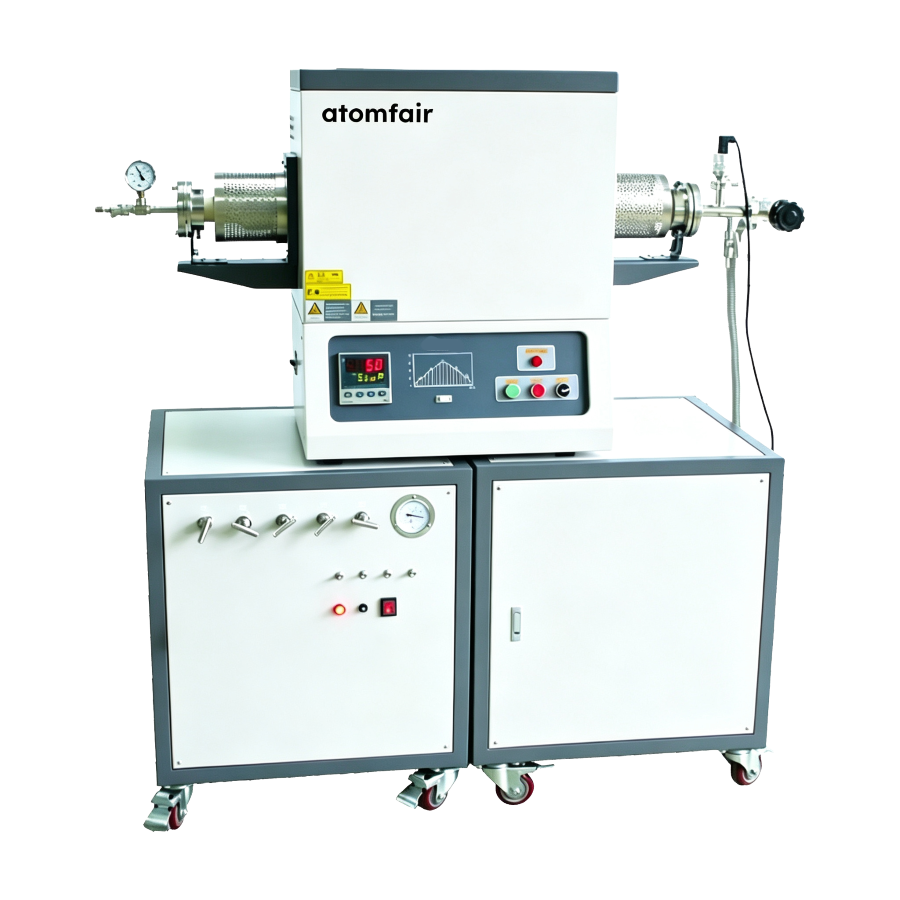
Single-Zone Sliding CVD System 1200 °C CV-1200-1P ATOMFAIR®
$5,000.00 -
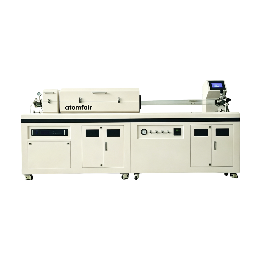
Single-Zone Sliding PECVD System 1200°C PV-1200-20 ATOMFAIR®
$29,000.00 -
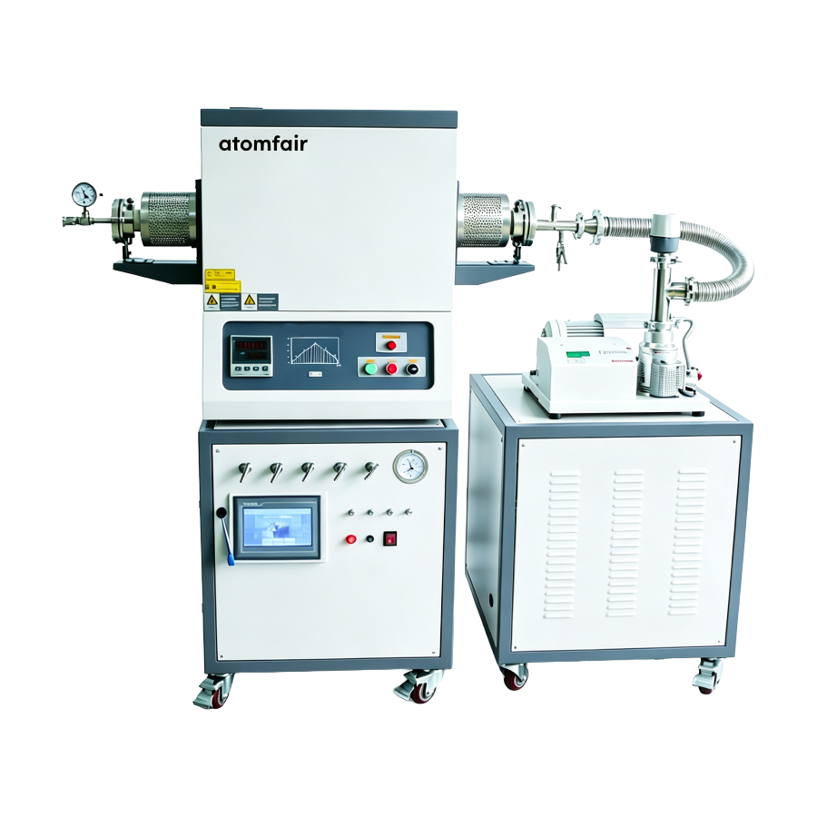
Sliding CVD System 1600 °C PECVD-Compatible ATOMFAIR®
$17,800.00 -
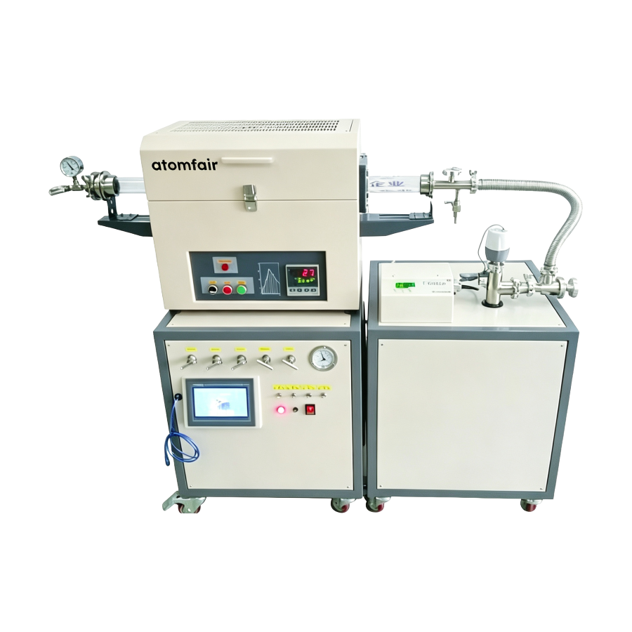
Sliding CVD System Graphene Growth 1200 °C ATOMFAIR®
$5,000.00 -
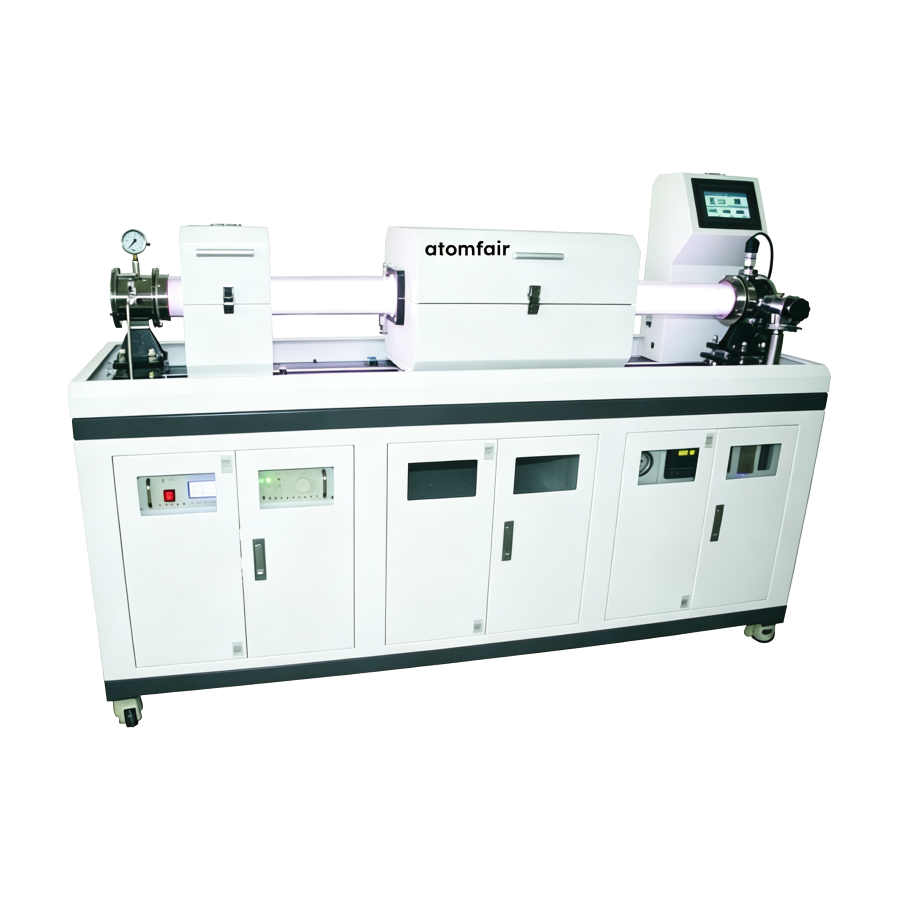
Small Intelligent PECVD System 150 W RF PV-1200-22 ATOMFAIR®
$25,000.00 -
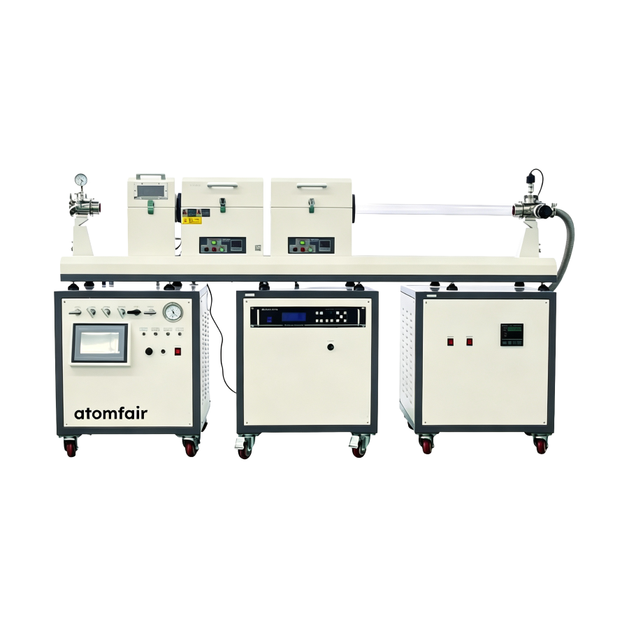
Small Sliding PECVD System 1200 °C 150 W RF ATOMFAIR®
$35,800.00 -
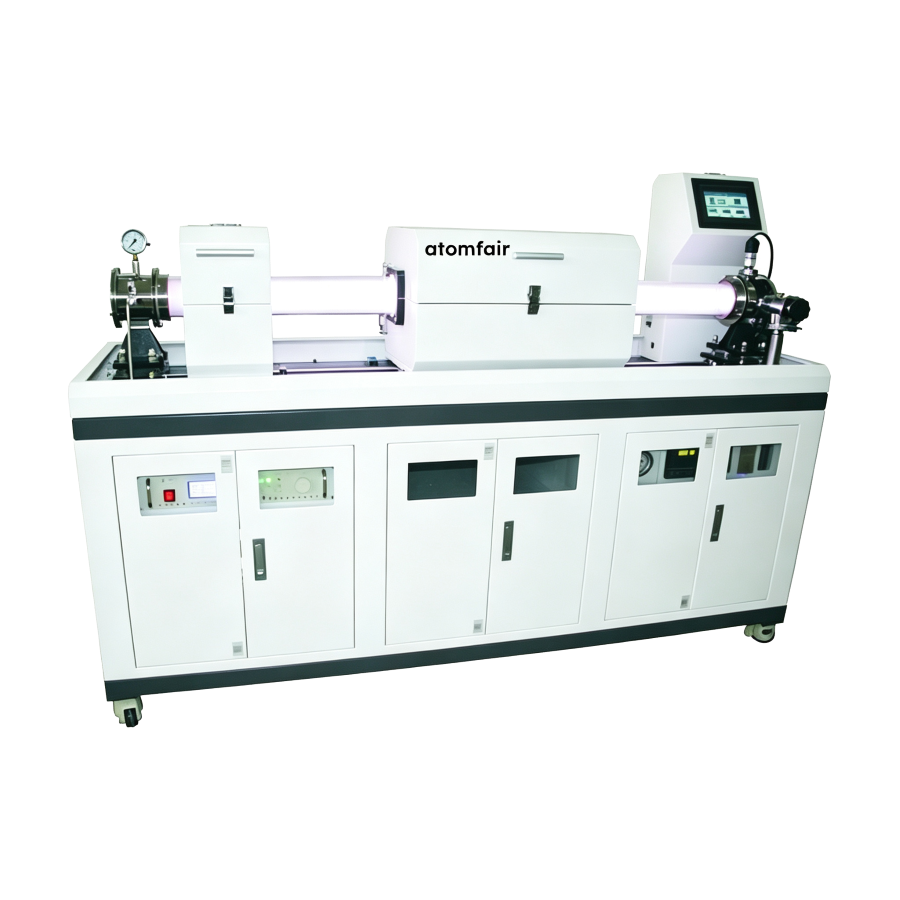
Three-Zone PECVD Lab System 1200 °C 500 W RF ATOMFAIR®
$42,000.00 -
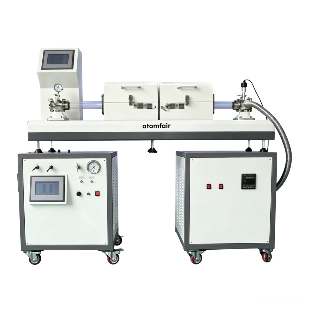
Two-Dimensional Materials Growth System 1200°C 4kW
$6,500.00