|
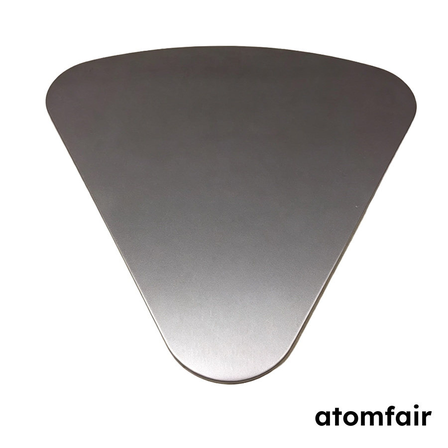
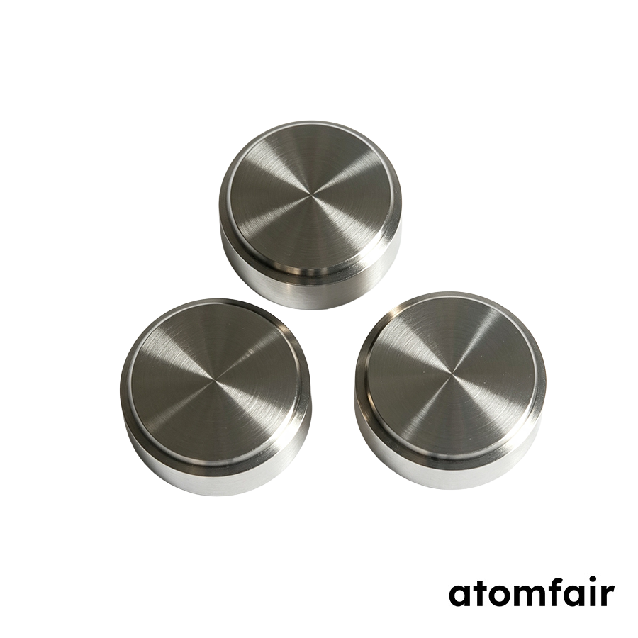
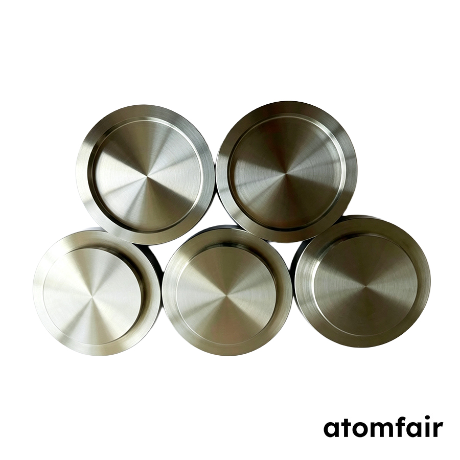
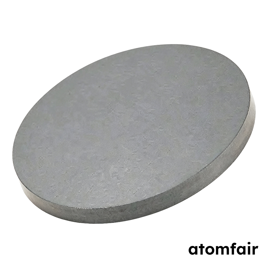
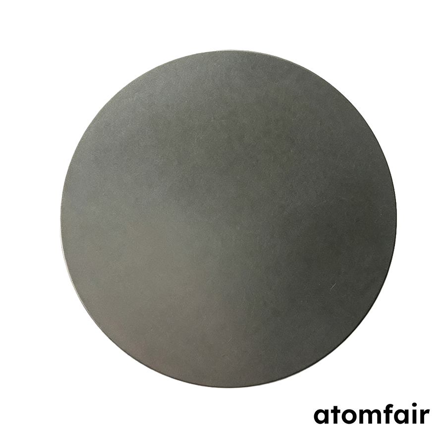
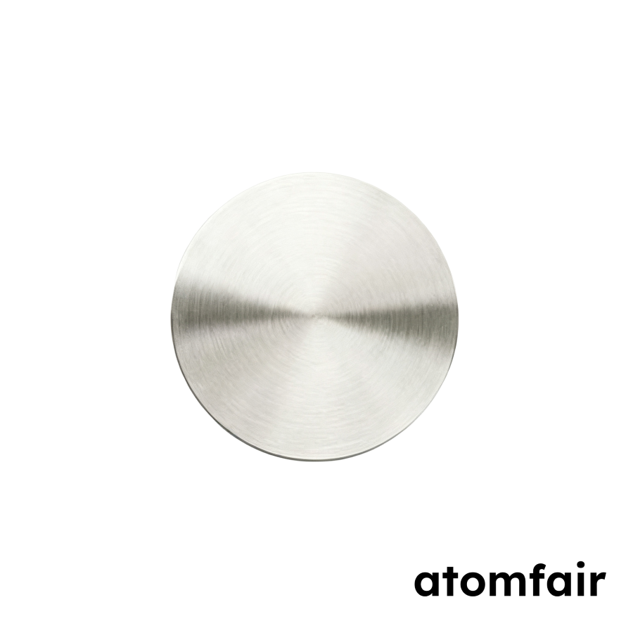
High Purity Tin Sputtering Target, 99.999%
Product Type: Round planar sputtering target
Research-grade laboratory product
|
|||||||||||||||||||||||||||||||||||||
|
|||||||||||||||||||||||||||||||||||||
|
LABORATORY PROCUREMENT SUPPORT
For model selection, accessory matching, platform compatibility or configuration confirmation, contact our technical sales team.
INQUIRY: inquiry@atomfair.com
|
|||||||||||||||||||||||||||||||||||||
|
Manufacturer: Atomfair LLC
Brand: ATOMFAIR®
|
The target must be stored in a dry, inert atmosphere to prevent surface oxidation that degrades sputtering performance. Vacuum packaging must remain sealed until installation to maintain specified purity and surface finish.
- Surface Oxidation Risk: Exposure to ambient air for extended periods may form a native oxide layer that requires pre-sputter cleaning or increased conditioning time.
- Mechanical Damage Sensitivity: The turned or ground surface finish (Ra ≤ 1.6 μm) is susceptible to scratches and contamination from improper handling or contact with hard surfaces.
- Bonding Interface Constraint: Unbonded targets require a compatible backing plate and bonding method to ensure thermal and electrical contact during sputtering.
This procedure covers unpacking, mounting, and conditioning a round planar tin sputtering target in a standard magnetron sputtering system. Proper installation prevents contamination and ensures uniform film deposition.
Required Equipment: Cleanroom gloves, Isopropyl alcohol and lint-free wipes, Torque wrench with compatible screwdriver bit
- Inspect vacuum packaging
Inspect the vacuum-sealed packaging for any breaches or damage before opening to confirm the target has not been exposed to ambient atmosphere. - Clean target surface
Wipe the target surface gently with isopropyl alcohol and a lint-free wipe to remove any particulate contamination from handling. - Mount target on backing plate
Secure the target onto the backing plate using the specified fasteners, tightening to the manufacturer's recommended torque to ensure uniform thermal contact. - Install assembly in sputter chamber
Transfer the mounted assembly into the sputter chamber and secure it according to the system's installation procedure. - Evacuate chamber and pre-sputter
Evacuate the chamber to base pressure, then pre-sputter the target for at least 5 minutes with the shutter closed to remove any surface oxide layer.
What is the maximum total critical impurity level for the Atomfair 99.999% tin sputtering target, and how does it affect film purity in transparent conductive oxide deposition?
The typical total critical impurities are ≤10 ppm, as specified for the Sn 4N5 material grade with 99.999% purity. This low impurity threshold minimizes contamination in transparent conductive and semiconductor films, ensuring controlled sputtering workflows for low-melting-point materials research.
Can this unbonded tin target be bonded to a copper backing plate, and what dimensional tolerances must be considered for integration into a standard sputter gun?
Yes, optional copper backing plate bonding is available. The target has a diameter tolerance of ±0.10 mm and thickness tolerance of ±0.10 mm (typical), which must be matched to the sputter gun's pocket dimensions. Available diameters range from 25.4 mm to 101.6 mm, and thicknesses from 3 mm to 6.35 mm, requiring configuration review before quotation.
What surface roughness and handling precautions are required for this 99.999% tin sputtering target to avoid oxidation or mechanical damage before installation?
The target surface is turned/ground to a typical Ra ≤1.6 μm. It is vacuum-packed with a Certificate of Analysis (COA) to prevent oxidation. Due to tin's low melting point and softness, careful handling is required to avoid scratches or deformation; final parameters are confirmed by batch inspection.
This 99.999% tin round planar sputtering target offers 7.31 g/cm3 density and 10.9 micro-ohm cm resistivity for transparent conductive and semiconductor film research, with a broad range of diameters and thicknesses but unbonded delivery and typical tolerances that must be confirmed during configuration.
Positive
- 99.999% purity with controlled impurities: The Sn 4N5 grade with 99.999% purity and <=10 ppm typical total critical impurities supports controlled sputtering workflows for transparent conductive and semiconductor film deposition.
- Broad size range for chamber fit: Available thicknesses from 3 mm to 6.35 mm and diameters from 25.4 mm to 101.6 mm allow configuration of the round planar target for different sputter sources while retaining the same high-purity material system.
Trade-offs
- Unbonded by default requires bonding decision: The target is supplied unbonded unless Cu backing plate bonding is selected, so the user must arrange backing plate integration or clamping compatible with the sputter cathode before deposition.
- Tolerances are typical and configuration-dependent: Diameter and thickness tolerance of +/-0.10 mm are listed as typical, and final parameters are confirmed only by batch inspection and the agreed configuration, requiring explicit pre-order confirmation for cathodes with tight dimensional constraints.
Every advanced material, component, equipment, and instrument in our catalog is backed by rigorous testing. We maintain strict internal quality management frameworks and align with CE conformity metrics to deliver transparent, reproducible performance data via our public open-science repository.
To request raw batch performance data, submit formal vendor registration paperwork, or execute a fast-turnaround R&D manufacturing loop, contact us at inquiry@atomfair.com.
Item is dispatched under the Atomfair Shipping & Delivery Framework (Free worldwide shipping on orders over $59 USD excl. heavy equipment). Return is governed by the Atomfair Return & Refund Policy (7-day technical return window).