|
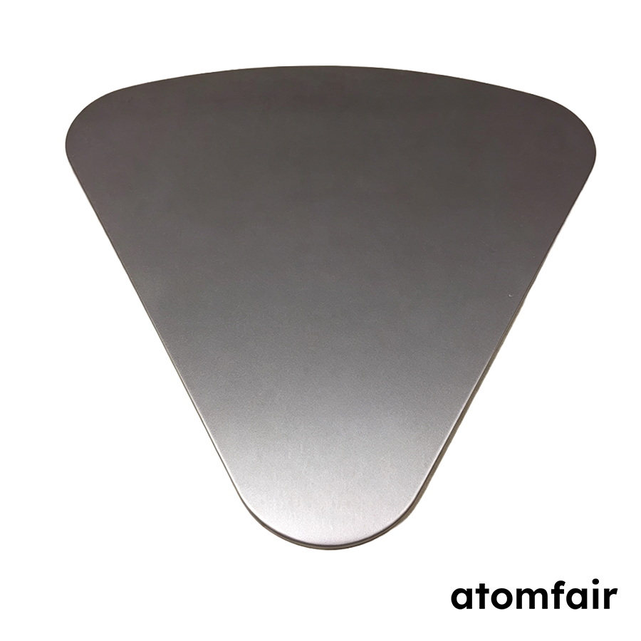
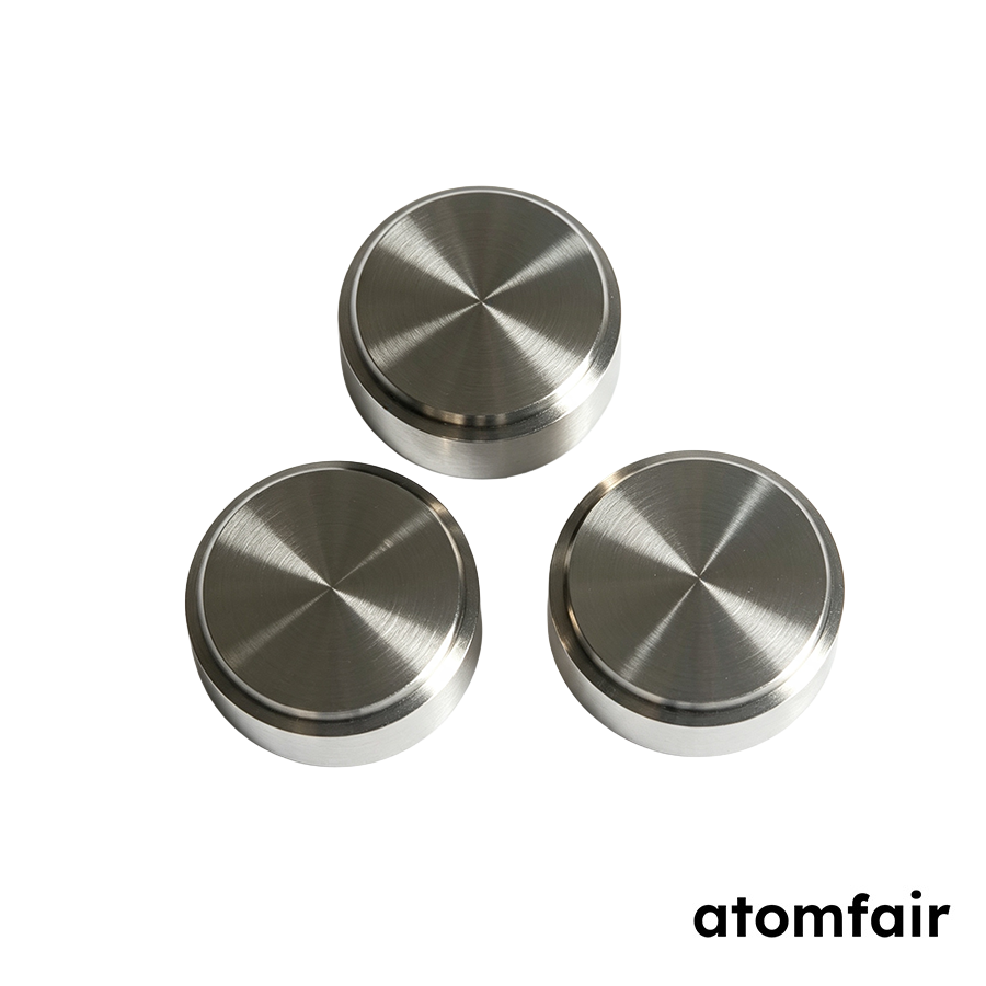
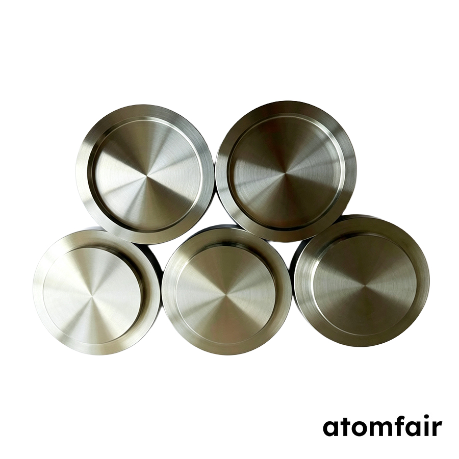
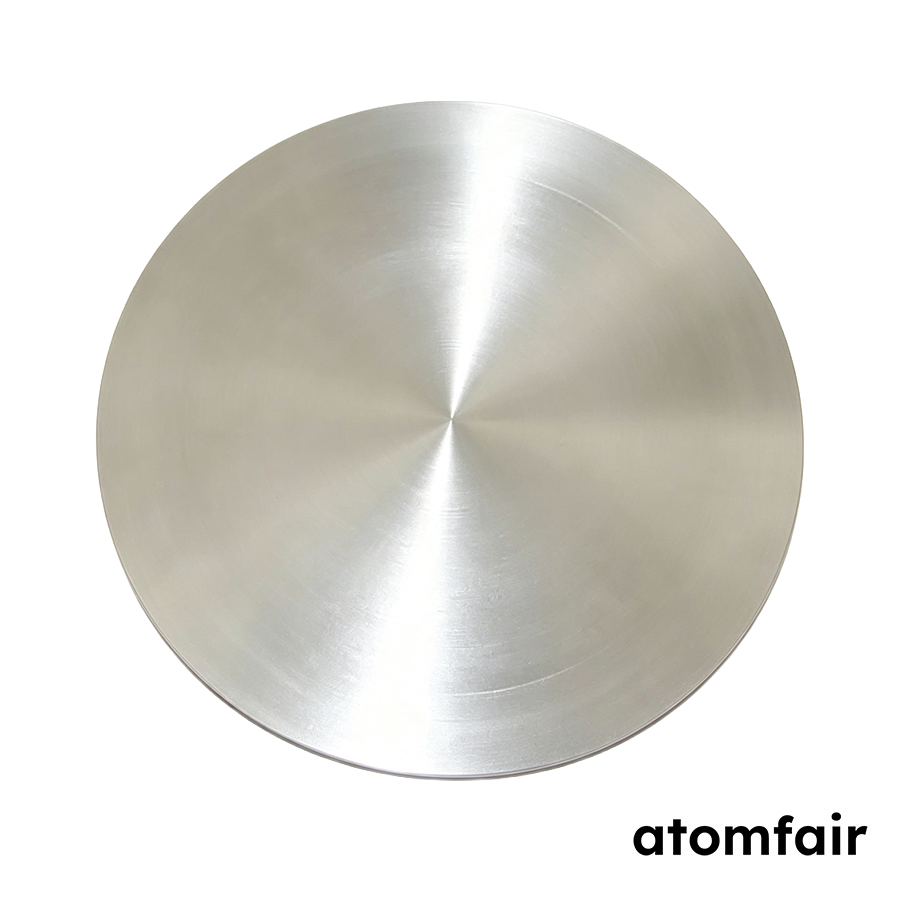
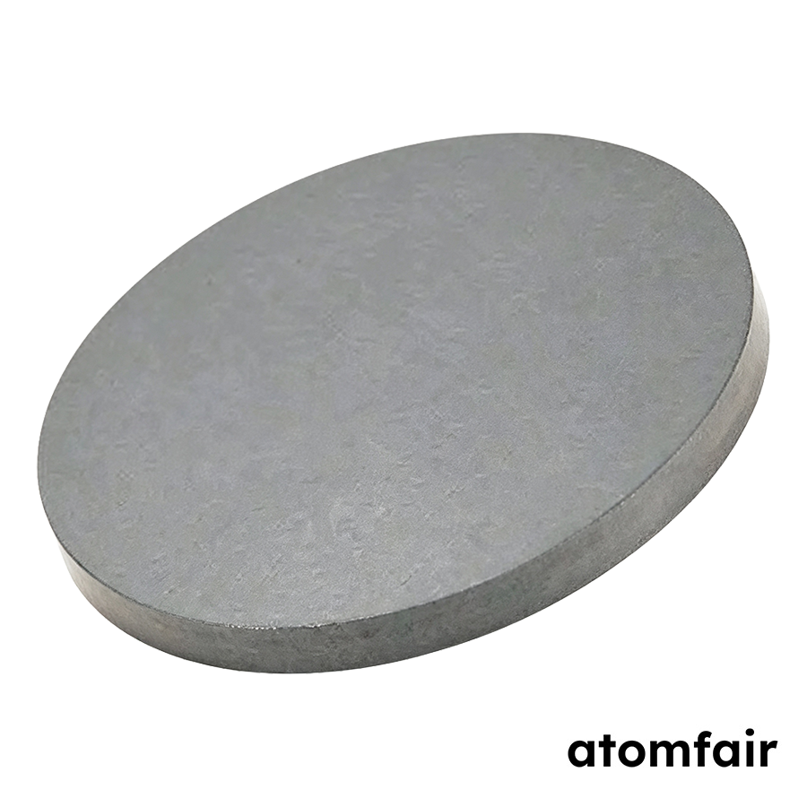
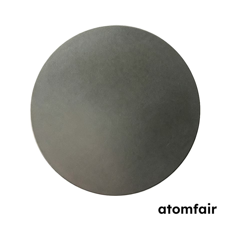
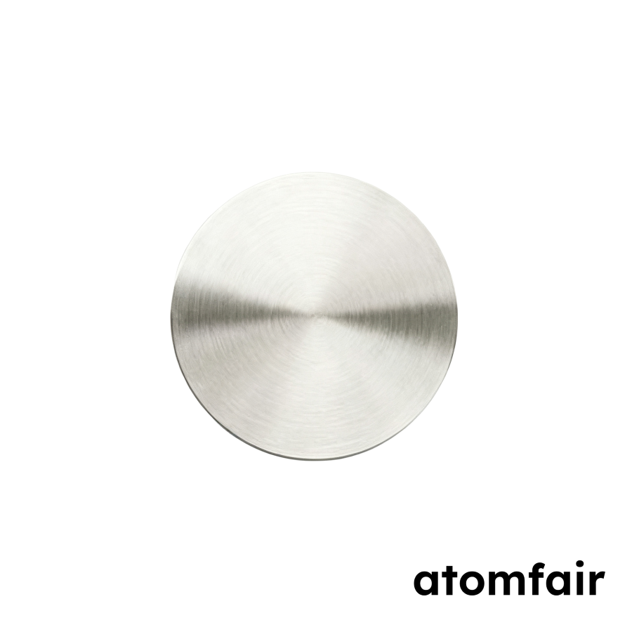
High Purity Tin Sputtering Target, 99.99%
Product Type: Round planar sputtering target
Research-grade laboratory product
|
|||||||||||||||||||||||||||||||||||||
|
|||||||||||||||||||||||||||||||||||||
|
LABORATORY PROCUREMENT SUPPORT
For model selection, accessory matching, platform compatibility or configuration confirmation, contact our technical sales team.
INQUIRY: inquiry@atomfair.com
|
|||||||||||||||||||||||||||||||||||||
|
Manufacturer: Atomfair LLC
Brand: ATOMFAIR®
|
This document specifies storage, handling, and mounting constraints for the 99.99% tin round planar sputtering target. Following these constraints preserves the as-supplied surface condition and dimensional fit before installation.
- Vacuum storage: Store the target in its vacuum-sealed packaging with the certificate of analysis until immediately before installation.
- Surface preservation: Preserve the as-supplied turned or ground surface finish by avoiding direct contact with the sputtering face during handling and mounting.
- Bonding configuration: Confirm whether the target is configured unbonded or with the optional Cu backing plate before mounting, because bonding affects the required backing setup.
- Configuration verification: Verify that the batch-inspected dimensions and parameters match the agreed configuration before installation.
What is the typical total critical impurity level for the 99.99% tin sputtering target and how does it affect film resistivity?
The typical total critical impurities are ≤100 ppm. This high purity minimizes contamination in deposited films, which is crucial for transparent conductive and semiconductor applications where trace impurities can alter electrical properties. The target's electrical resistivity is 10.9 micro-ohm cm at this purity grade.
What bonding options are available for this tin sputtering target and how does bonding affect thermal management during sputtering?
The target is available unbonded or with optional backplate bonding. Unbonded targets are suitable for direct mounting, while backplate bonding improves thermal contact with the sputter cathode, enhancing heat dissipation during high-power sputtering of low-melting-point tin. This helps prevent target cracking or melting under sustained operation.
How should the 99.99% tin sputtering target be stored and handled to maintain surface integrity?
The target is vacuum packed with a Certificate of Analysis to prevent oxidation and contamination. The surface is prepared by turning/grinding to Ra≤1.6 μm, so handling should avoid scratches or debris. Storage in a dry, inert environment is recommended to preserve the surface state before installation.
This 99.99% purity tin sputtering target (Sn 3N5 grade) offers a round planar geometry with a typical surface finish of Ra≤1.6 μm and tight dimensional tolerances (±0.10 mm), making it suitable for transparent conductive and semiconductor film deposition. Its low electrical resistivity (10.9 μΩ·cm) and density of 7.31 g/cm³ support controlled sputtering workflows, though the unbonded default and low melting point require careful handling and optional backing plate bonding for thermal management.
Positive
- High purity with controlled impurities: The 99.99% purity grade (Sn 3N5) with typical total critical impurities ≤100 ppm ensures minimal contamination in sensitive sputtering applications such as transparent conductive and semiconductor films.
- Precision surface and dimensional tolerances: A typical surface finish of Ra≤1.6 μm and dimensional tolerances of ±0.10 mm for diameter and thickness support reproducible deposition conditions and consistent target performance across the available thickness and diameter configurations.
Trade-offs
- Unbonded default requires bonding option: The target ships unbonded; for effective thermal management during sputtering, buyers must select the optional Cu backing plate bonding, which adds a configuration step and potential lead time.
- Low melting point material constraints: Tin's low melting point (as implied by the 'low-melting-point materials research' application) requires careful handling and controlled sputtering parameters to avoid thermal damage or target deformation, especially at higher power densities.
Every advanced material, component, equipment, and instrument in our catalog is backed by rigorous testing. We maintain strict internal quality management frameworks and align with CE conformity metrics to deliver transparent, reproducible performance data via our public open-science repository.
To request raw batch performance data, submit formal vendor registration paperwork, or execute a fast-turnaround R&D manufacturing loop, contact us at inquiry@atomfair.com.
Item is dispatched under the Atomfair Shipping & Delivery Framework (Free worldwide shipping on orders over $59 USD excl. heavy equipment). Return is governed by the Atomfair Return & Refund Policy (7-day technical return window).