|
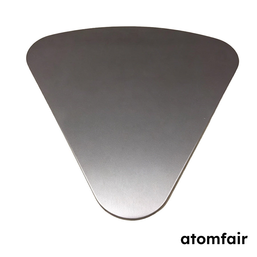
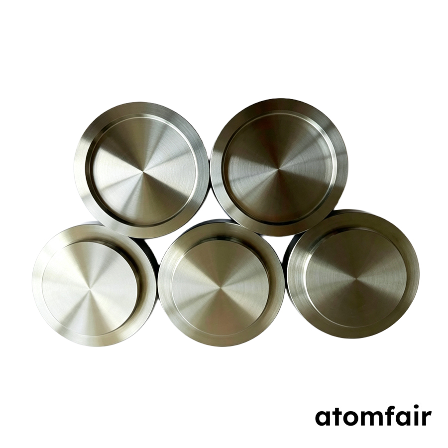
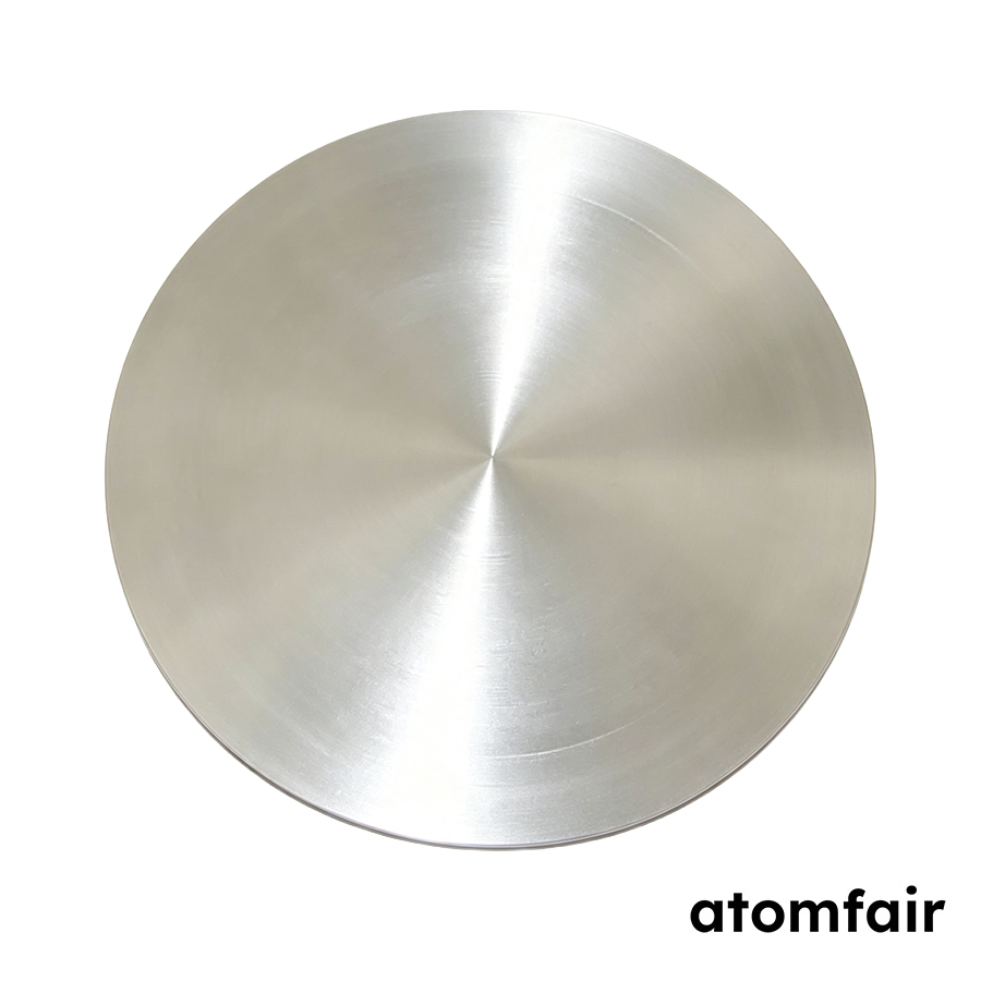
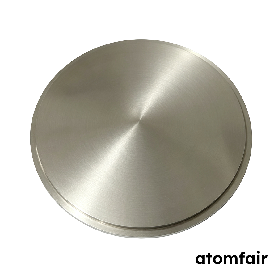
High Purity Silicon Sputtering Target, 99.999%
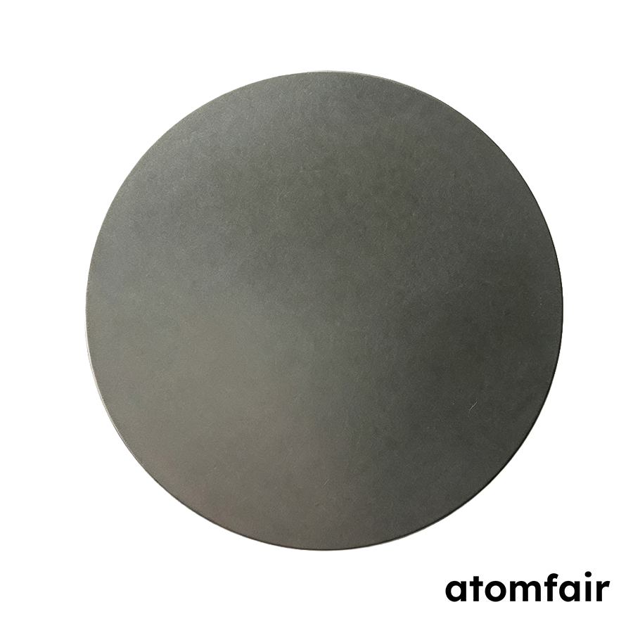
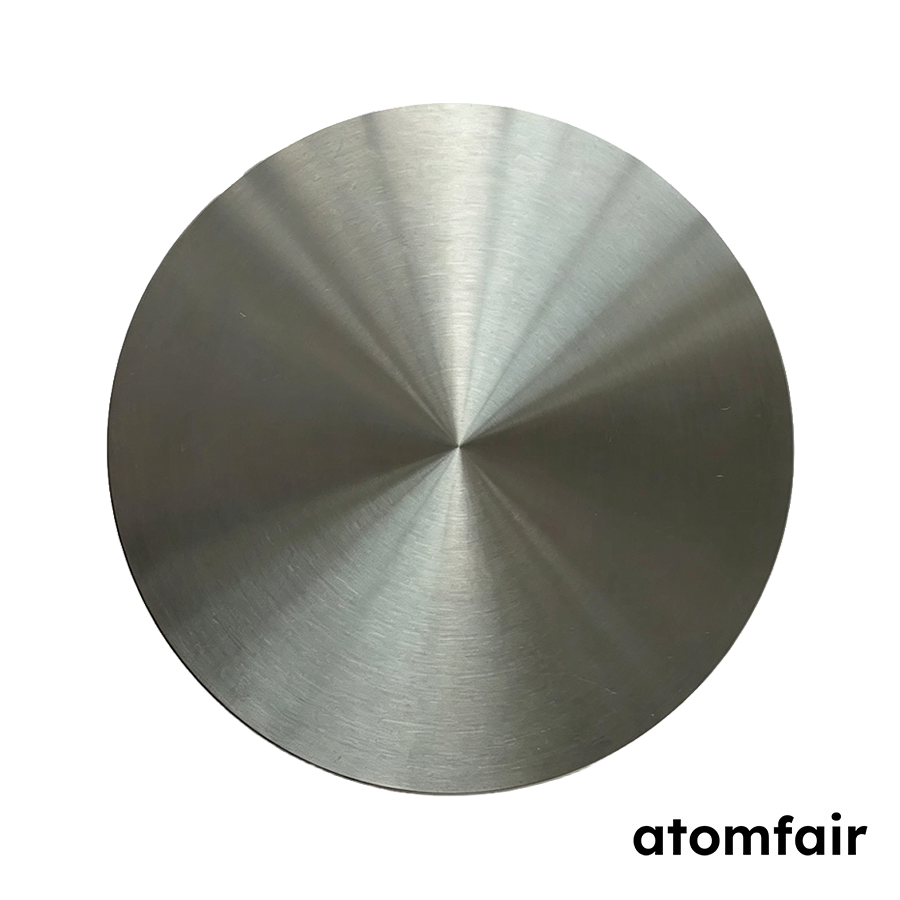
Product Type: Round planar sputtering target
Research-grade laboratory product
|
|||||||||||||||||||||||||||||||||||||
|
|||||||||||||||||||||||||||||||||||||
|
LABORATORY PROCUREMENT SUPPORT
For model selection, accessory matching, platform compatibility or configuration confirmation, contact our technical sales team.
INQUIRY: inquiry@atomfair.com
|
|||||||||||||||||||||||||||||||||||||
|
Manufacturer: Atomfair LLC
Brand: ATOMFAIR®
|
Silicon sputtering targets require verification of surface condition, dimensional tolerance, bonding configuration, and storage atmosphere before installation. Uncontrolled handling or incompatible mounting can lead to contamination, mechanical mismatch, or deposition process failure.
- Surface condition verification: Confirm the turned or ground target surface maintains a typical Ra of no more than 1.6 µm before installation.
- Dimensional tolerance check: Verify the target diameter and thickness remain within the stated ±0.10 mm tolerance against the sputter tool's holder specifications.
- Bonding configuration selection: Choose unbonded, copper backing plate bonded, or magnetic shim mounting only after confirming compatibility with the deposition system's clamping and cooling design.
- Storage and packaging retention: Keep the target in its vacuum packaging until mounting to limit surface contamination and oxidation.
- Resistivity grade compatibility: Confirm the doping and resistivity grade, whether intrinsic, n-type, or p-type, matches the intended sputtering process requirements.
How does the electrical resistivity of the 99.999% silicon sputtering target change with doping, and what resistivity values are specified?
Electrical resistivity varies with doping/resistivity grade; intrinsic Si is approximately 2.3×10^5 ohm cm. The target is offered as Si 4N5 intrinsic, n-type, or p-type, so the resistivity grade must be selected to match the intended sputtering process. Purity is 99.999% with typical total critical impurities <=10 ppm.
What dimensional tolerances, bonding options, and diameters are available for integrating this silicon target into a magnetron sputtering system?
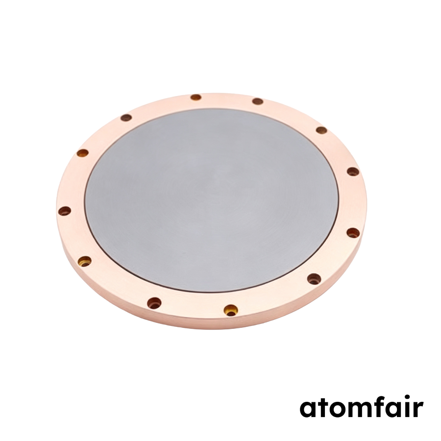
This round planar target is available in diameters of 25.4 mm, 50 mm, 50.8 mm, 60 mm, 76.2 mm, 80.0 mm, 101.6 mm, and 100 mm, with typical diameter tolerance +/-0.10 mm and thickness tolerance +/-0.10 mm. Thickness options are 3 mm, 4 mm, 5 mm, 6 mm, and 6.35 mm. Standard delivery is unbonded, with optional Cu backing plate bonding or magnetic shim available as a configured option.
How is the silicon target surface finished, packaged, and documented for laboratory use?
The surface state is turned/ground with Ra <=1.6 um typical. The target is vacuum packed with a certificate of analysis, and final parameters are confirmed by batch inspection and the agreed configuration. This packaging is intended to protect the research-grade surface during storage and handling.
This 99.999% round planar silicon sputtering target provides low typical total critical impurities (≤10 ppm), a turned/ground surface (Ra≤1.6 µm), and a broad diameter/thickness matrix for magnetron sputtering of semiconductor films. Resistivity varies with doping/resistivity grade, and the target ships unbonded unless an optional Cu backing plate or magnetic shim is configured, so process and mounting requirements must be confirmed before ordering.
Positive
- 99.999% purity, ≤10 ppm critical impurities: The 99.999% silicon grade with typical total critical impurities ≤10 ppm supports controlled sputtering workflows for semiconductor film and silicon-based device deposition.
- Broad round planar size matrix: Round planar geometry is available in diameters from 25.4 mm to 101.6 mm and thicknesses from 3 mm to 6.35 mm, accommodating different magnetron sputtering cathode dimensions and target lifetimes.
Trade-offs
- Resistivity varies with doping grade: Electrical resistivity is not fixed; it changes with doping/resistivity grade, with intrinsic Si at approximately 2.3×10^5 ohm cm. The correct grade must be selected to match the sputtering power source and deposition process.
- Unbonded by default; mounting must be confirmed: Targets are supplied unbonded unless optional Cu backing plate bonding or a magnetic shim is specified, so the sputter gun's mechanical and thermal interface requirements must be confirmed before ordering.
Every advanced material, component, equipment, and instrument in our catalog is backed by rigorous testing. We maintain strict internal quality management frameworks and align with CE conformity metrics to deliver transparent, reproducible performance data via our public open-science repository.
To request raw batch performance data, submit formal vendor registration paperwork, or execute a fast-turnaround R&D manufacturing loop, contact us at inquiry@atomfair.com.
Item is dispatched under the Atomfair Shipping & Delivery Framework (Free worldwide shipping on orders over $59 USD excl. heavy equipment). Return is governed by the Atomfair Return & Refund Policy (7-day technical return window).