|
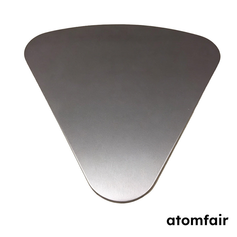
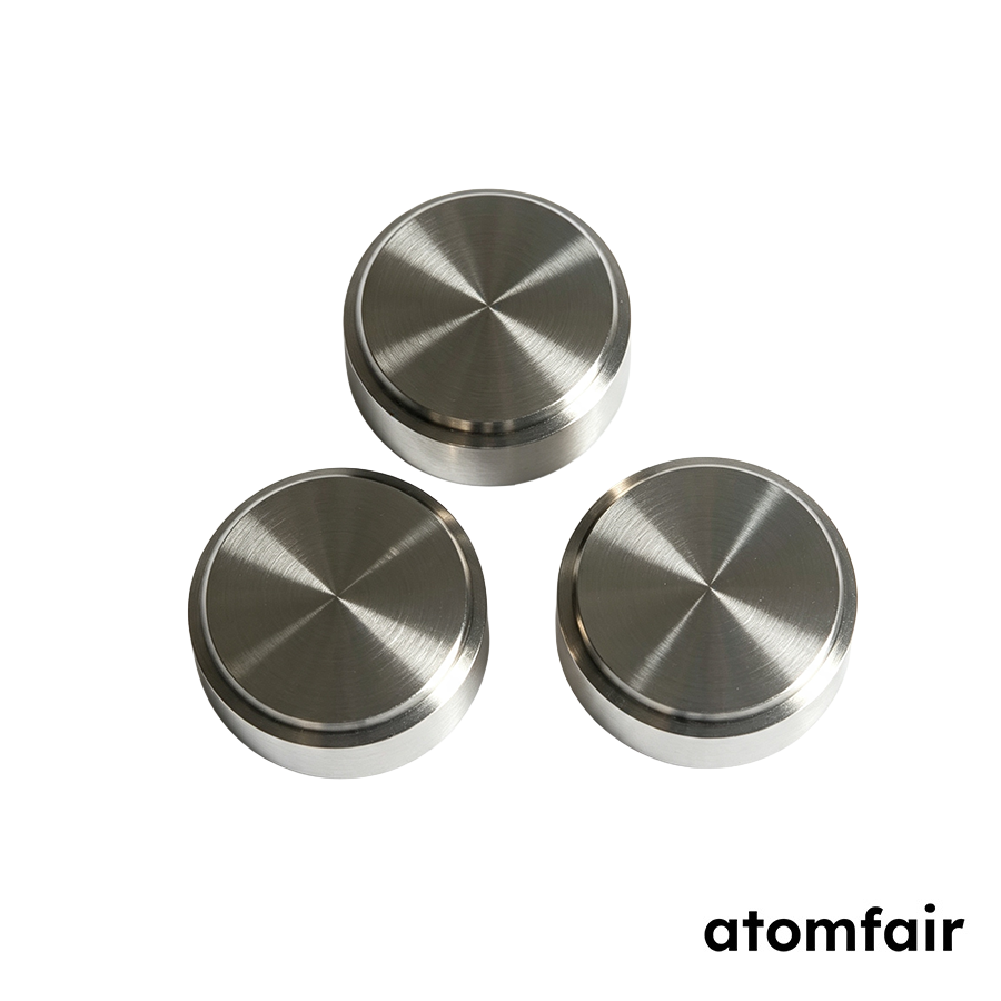
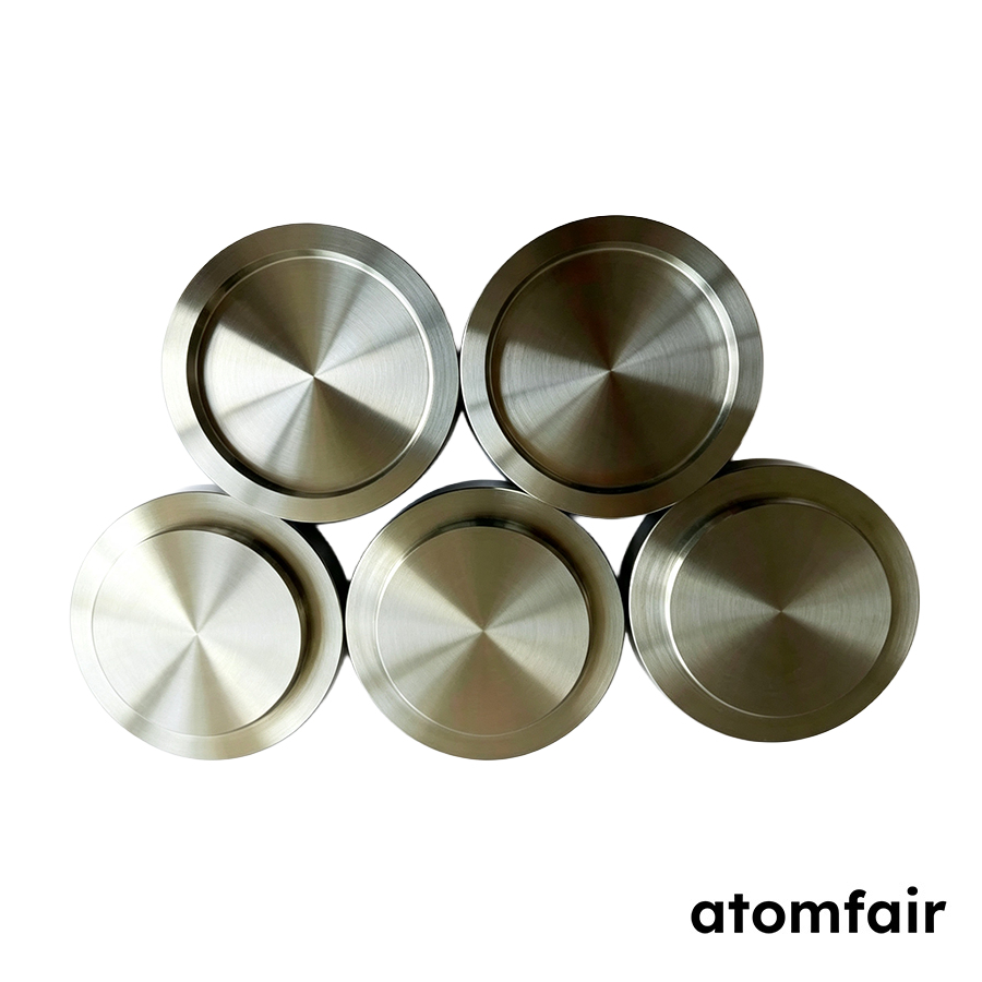
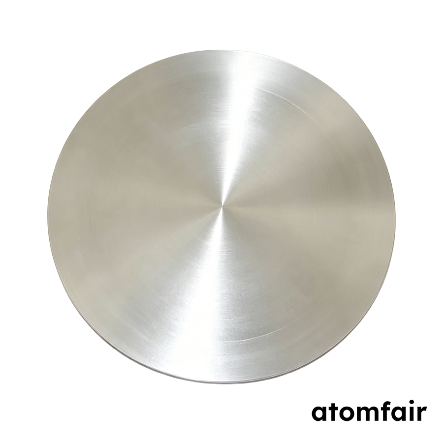
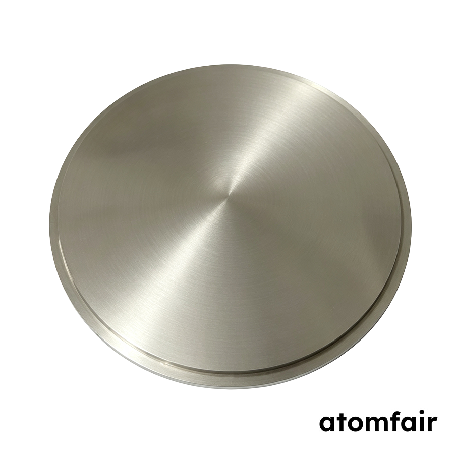
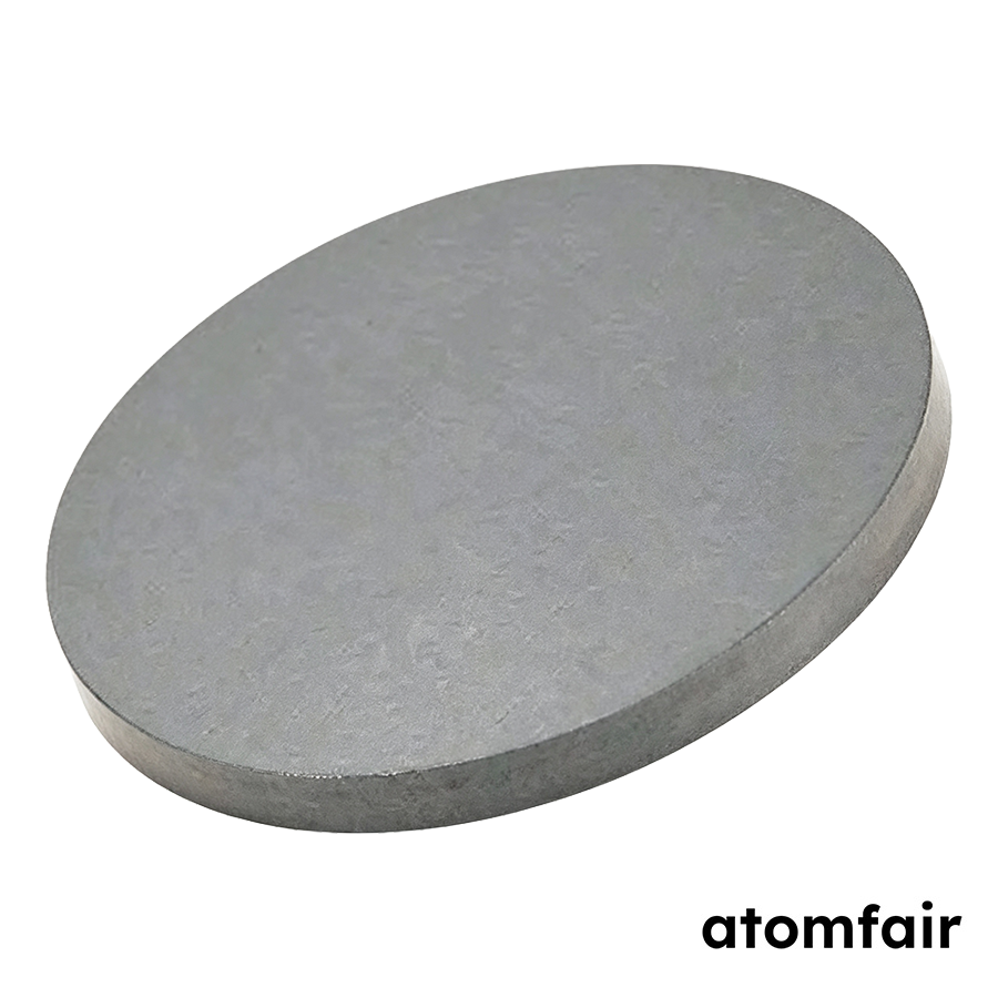
High Purity Lead Sputtering Target, 99.999%
Product Type: Round planar sputtering target
Research-grade laboratory product
|
|||||||||||||||||||||||||||||||||||||
|
|||||||||||||||||||||||||||||||||||||
|
LABORATORY PROCUREMENT SUPPORT
For model selection, accessory matching, platform compatibility or configuration confirmation, contact our technical sales team.
INQUIRY: inquiry@atomfair.com
|
|||||||||||||||||||||||||||||||||||||
|
Manufacturer: Atomfair LLC
Brand: ATOMFAIR®
|
Store the target in a vacuum-sealed package with desiccant to prevent surface oxidation and contamination. Avoid exposure to moisture and ambient air prior to installation to maintain the specified surface roughness and purity.
- Surface Oxidation Risk: Lead oxidizes rapidly in air, forming a non-conductive layer that degrades sputtering performance and film purity.
- Mechanical Handling Constraint: The target is soft and easily scratched or deformed; handle only by the edges using clean, powder-free gloves.
- Bonding Consideration: Unbonded targets require a compatible backing plate and thermal interface material to ensure adequate heat dissipation during sputtering.
Install the target into a compatible sputter gun using a clean, unbonded backing plate with thermal paste. Condition the target surface by pre-sputtering at low power to remove any native oxide layer before film deposition.
Required Equipment: Clean, lint-free gloves, Isopropyl alcohol and wipes, Thermal paste or conductive foil
- Inspect the target
Inspect the target surface for scratches, dents, or discoloration before installation. - Clean the backing plate
Clean the backing plate surface with isopropyl alcohol and a lint-free wipe to remove any residues. - Apply thermal interface material
Apply a thin, even layer of thermal paste or place a conductive foil on the backing plate to ensure thermal contact. - Mount the target
Mount the target onto the backing plate, centering it carefully, and secure it with the sputter gun clamp or screws. - Pump down the chamber
Pump down the sputtering chamber to a base pressure below 5e-6 Torr to minimize residual gas contamination. - Pre-sputter the target
Pre-sputter the target at 10-20% of the intended deposition power for 5-10 minutes with the shutter closed to remove the surface oxide layer. - Verify the plasma
Verify a stable, uniform plasma before opening the shutter to begin film deposition.
How does the 99.999% purity and 20.6 micro-ohm cm electrical resistivity of the ATOMFAIR lead sputtering target influence film quality in semiconductor applications?
The 99.999% purity (≤10 ppm total critical impurities) ensures minimal contamination during sputtering, directly impacting film purity and device performance. The 20.6 micro-ohm cm electrical resistivity is characteristic of high-purity lead and supports consistent deposition rates for low-melting-point and semiconductor functional film research.
What bonding options are available for the ATOMFAIR lead sputtering target, and how do they affect integration with different sputtering systems?
The target is available unbonded or with optional Cu backing plate bonding. The dimensional tolerance of diameter+/-0.10 mm and thickness+/-0.10 mm ensures compatibility with standard sputtering system fixtures. Bonding choice should be matched to system thermal management requirements and target mounting design.
What is the standard packaging and documentation provided with the ATOMFAIR high-purity lead sputtering target?
The target is vacuum packed with a Certificate of Analysis (COA). The surface is prepared by turning or grinding to Ra≤1.6 µm typical. This packaging protects the target during transport and storage, and the COA confirms batch-specific purity and critical impurity levels.
This 99.999% Pb 4N5 round planar sputtering target (Atomfair Model AF-PB-99N999) provides low total critical impurities, defined dimensional tolerances, and a machined surface finish suitable for controlled semiconductor/functional-film research, while requiring configuration review of unbonded mounting and batch-confirmed final parameters.
Positive
- 99.999% Pb 4N5 purity with low critical impurities: The Pb 4N5 grade has a typical total critical impurity level of <=10 ppm, supporting contamination-sensitive sputtering workflows for low-melting-point materials, semiconductor films, and functional film research.
- Controlled round planar dimensions and surface finish: Diameter and thickness tolerances of +/-0.10 mm with a turned/ground surface of Ra<=1.6 um typical provide predictable target-to-cathode fit and a reproducible sputtering surface across the listed diameter and thickness configurations.
Trade-offs
- Unbonded standard mounting requires thermal interface planning: The listed bonding is unbonded, with optional Cu backing plate bonding only if specified; users must confirm the cathode mounting and thermal interface for this low-melting-point lead material before quotation.
- Final parameters confirmed only after batch inspection: Surface finish and dimensional values are stated as typical, and final parameters are confirmed by batch inspection and the agreed configuration, so final COA values must be reviewed before use in tight-tolerance systems.
Every advanced material, component, equipment, and instrument in our catalog is backed by rigorous testing. We maintain strict internal quality management frameworks and align with CE conformity metrics to deliver transparent, reproducible performance data via our public open-science repository.
To request raw batch performance data, submit formal vendor registration paperwork, or execute a fast-turnaround R&D manufacturing loop, contact us at inquiry@atomfair.com.
Item is dispatched under the Atomfair Shipping & Delivery Framework (Free worldwide shipping on orders over $59 USD excl. heavy equipment). Return is governed by the Atomfair Return & Refund Policy (7-day technical return window).