|
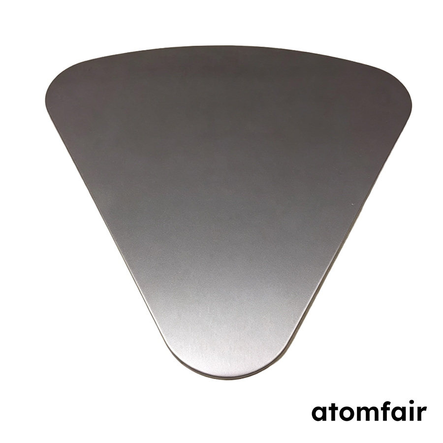
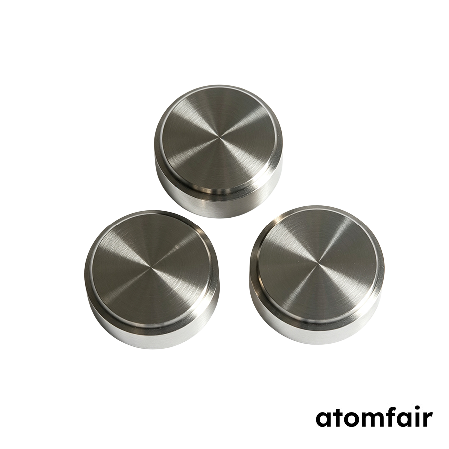
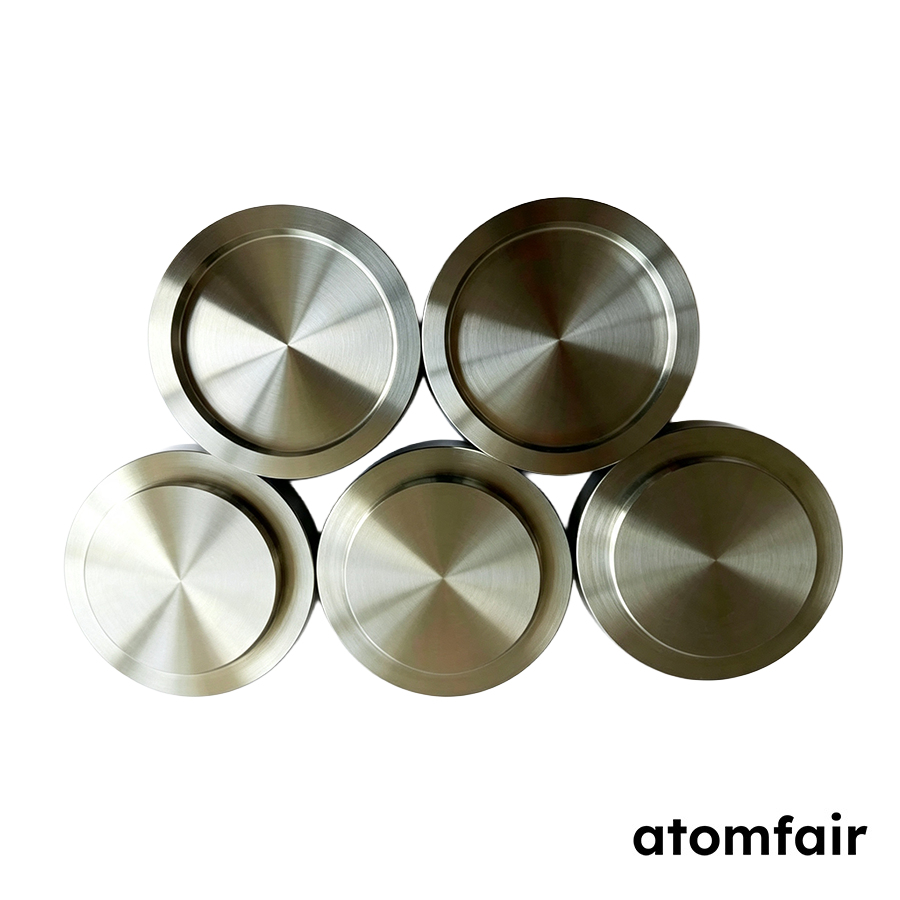
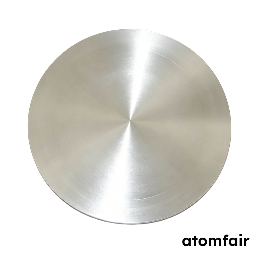
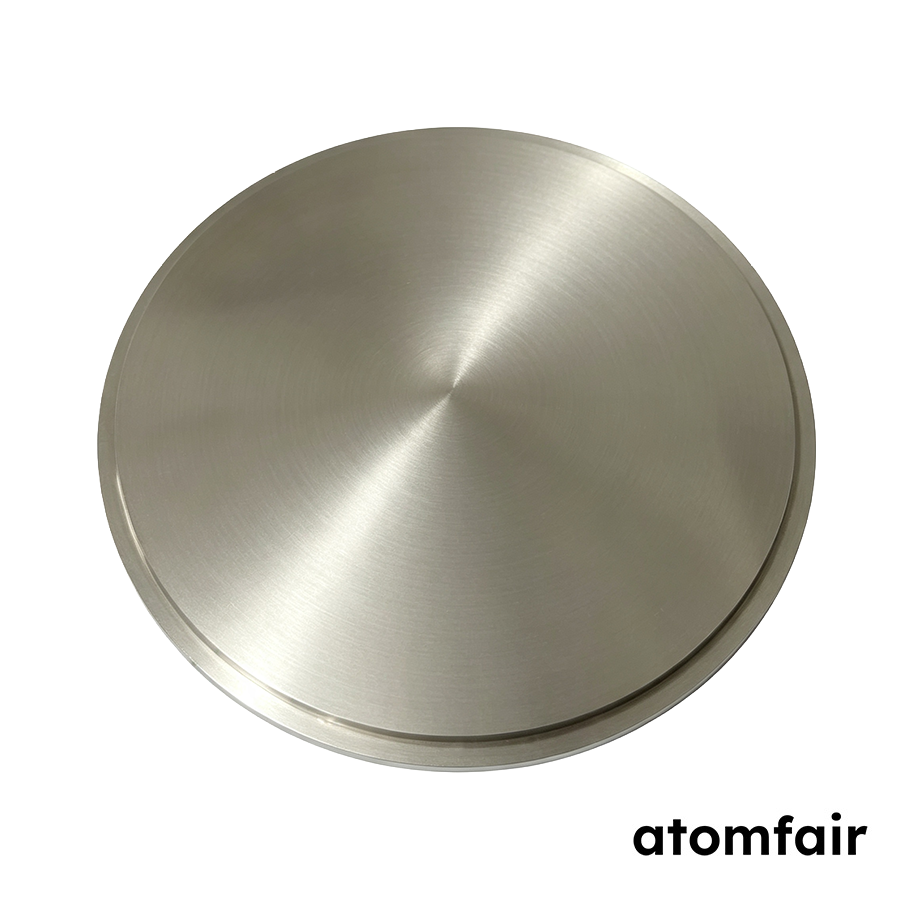
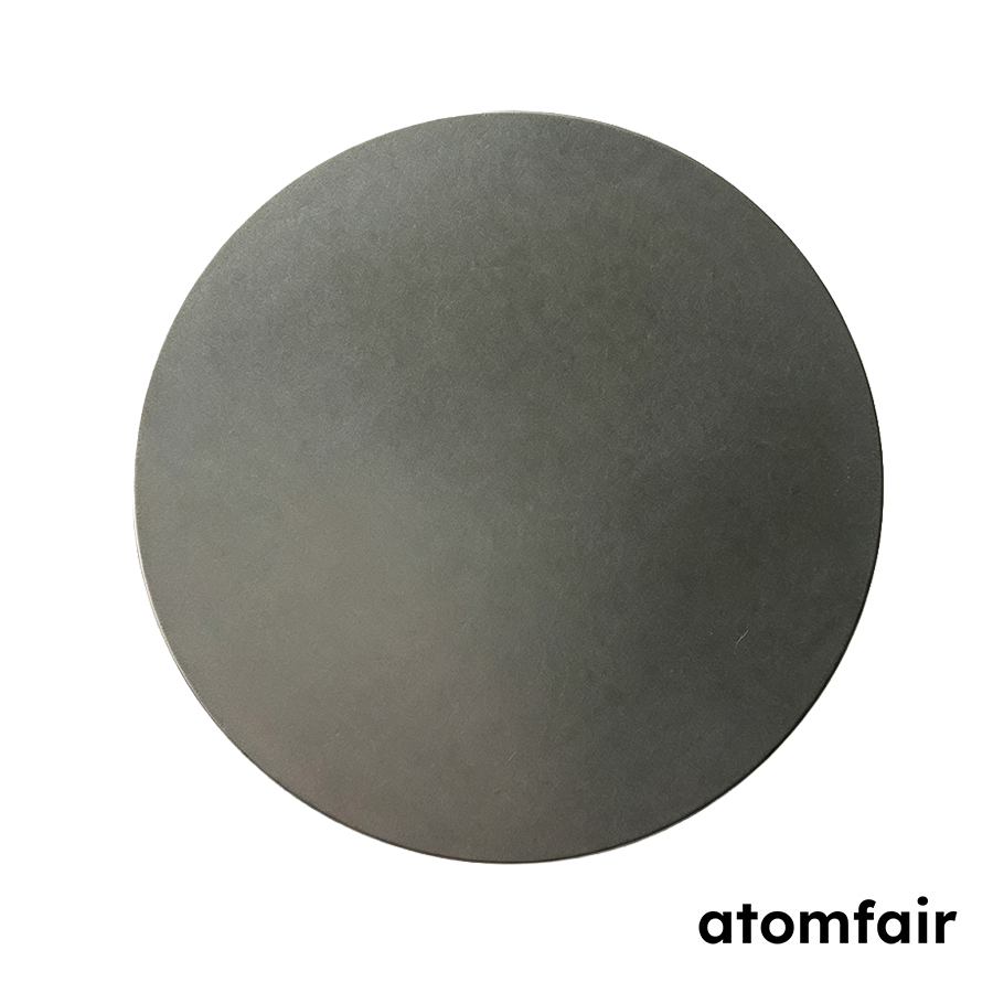
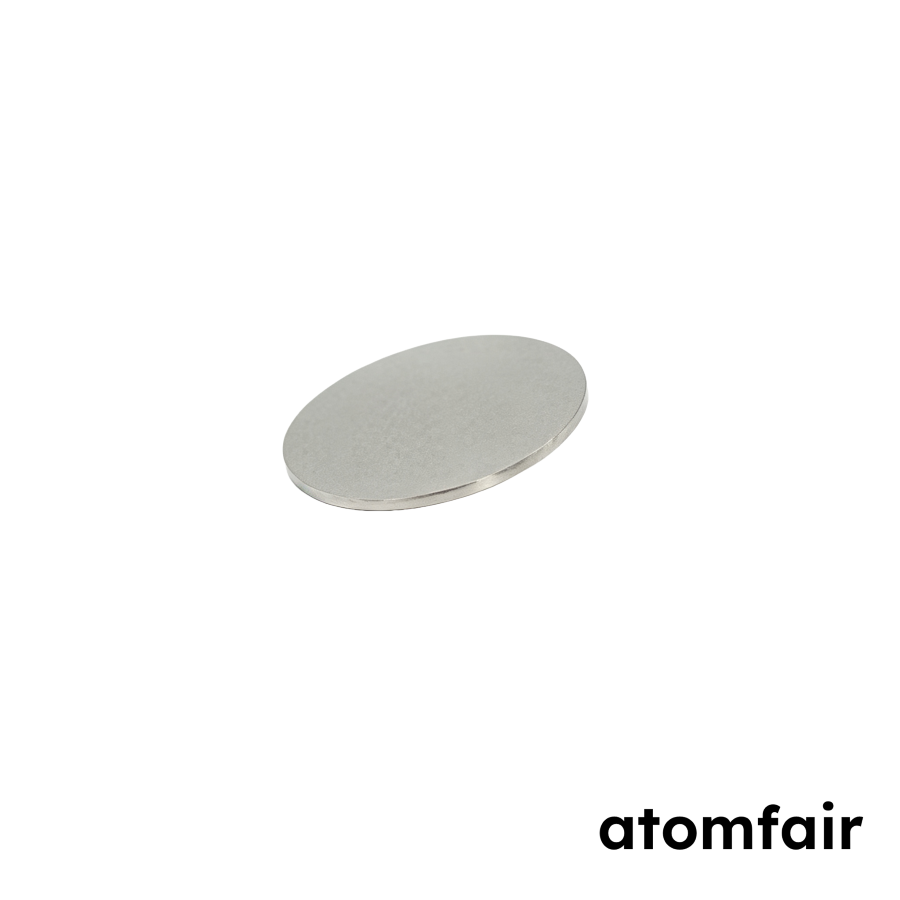
High Purity Bismuth Sputtering Target, 99.99%
Product Type: Round planar sputtering target
Research-grade laboratory product
|
|||||||||||||||||||||||||||||||||||||
|
|||||||||||||||||||||||||||||||||||||
|
LABORATORY PROCUREMENT SUPPORT
For model selection, accessory matching, platform compatibility or configuration confirmation, contact our technical sales team.
INQUIRY: inquiry@atomfair.com
|
|||||||||||||||||||||||||||||||||||||
|
Manufacturer: Atomfair LLC
Brand: ATOMFAIR®
|
This bismuth sputtering target is vacuum packed with a certificate of analysis to prevent oxidation during storage. The material exhibits low melting point and high electrical resistivity, requiring careful handling to avoid contamination or mechanical damage.
- Storage and Handling: Store the vacuum-sealed target in a dry, inert atmosphere to minimize surface oxidation before use.
- Surface Integrity: Maintain the as-machined surface finish (Ra ≤ 1.6 µm) by avoiding contact with abrasive or contaminating materials.
- Bonding Consideration: Confirm bonding requirements (unbonded, backing plate, or magnetic shim) prior to installation to ensure thermal and mechanical compatibility.
This procedure describes the safe installation and initial conditioning of a round planar bismuth sputtering target in a magnetron sputtering system. Proper handling prevents target cracking, contamination, or arcing during deposition.
Required Equipment: Cleanroom gloves, Vacuum-compatible mounting fixture, Sputtering system with inert gas supply
- Inspect the target
Inspect the target surface for visible defects, scratches, or contamination before removing the vacuum packaging. - Mount the target
Mount the target onto the sputtering cathode using the appropriate backing plate or bonding method, ensuring uniform thermal contact. - Evacuate the chamber
Evacuate the deposition chamber to a base pressure below 1×10⁻⁵ Torr to remove residual moisture and oxygen. - Pre-sputter the target
Pre-sputter the target for 5–10 minutes with the shutter closed to remove any surface oxide layer and stabilize the plasma. - Verify deposition parameters
Verify that the sputtering power, pressure, and gas flow are within the recommended range for bismuth to prevent target overheating.
What is the maximum total critical impurity level and how does it affect bismuth sputtering target performance?
The bismuth sputtering target is specified with a purity of 99.99% (Bi 3N5 grade) and typical total critical impurities of ≤100 ppm. This controlled impurity level is critical for thermoelectric and semiconductor film deposition, where trace contaminants can alter carrier concentration, Seebeck coefficient, or film stoichiometry, leading to unpredictable device performance.
Can this bismuth target be bonded to a backing plate for magnetron sputtering, and what are the options?
Yes, the target is available unbonded, but optional Cu backing plate bonding or magnetic shim can be specified. This is particularly relevant for magnetron sputtering systems where thermal management and magnetic field distribution are critical; the unbonded option requires the user to handle mounting, while bonded configurations improve heat dissipation and target stability during high-power deposition.
What dimensional tolerances and surface finish are provided for this bismuth sputtering target?
The target is manufactured with a surface finish of Ra ≤ 1.6 μm (typical) via turning or grinding, and dimensional tolerances of ±0.10 mm for both diameter and thickness. These tolerances ensure compatibility with standard sputtering gun clamps and repeatable film thickness uniformity, which is essential for research-grade thin film deposition.
This 99.99% bismuth round planar sputtering target supports controlled thermoelectric/semiconductor film deposition through a defined purity cap, 106.8 micro-ohm cm resistivity, Ra<=1.6 um surfaces, and +/-0.10 mm dimensional tolerances, with diameter and thickness options for cathode matching; the default unbonded state requires the user to confirm backing plate bonding or magnetic shim and thermal management before deployment.
Positive
- Four-nines purity with impurity cap: The 99.99% material grade (Bi 3N5) and typical total critical impurities <=100 ppm support reproducible sputtering conditions for thermoelectric/semiconductor film deposition.
- Controlled surface and dimensional tolerances: Turning/grinding to Ra<=1.6 um and +/-0.10 mm diameter/thickness tolerances permit consistent target seating and predictable film thickness in magnetron sputtering setups.
Trade-offs
- Unbonded default requires mounting plan: The target ships unbonded, so users must specify backing plate bonding or magnetic shim and confirm cathode compatibility for thermal and magnetic management before use.
- Typical values need batch confirmation: Surface roughness and dimensional tolerances are stated as typical, with final parameters confirmed by batch inspection and the agreed configuration, requiring incoming QA verification.
Every advanced material, component, equipment, and instrument in our catalog is backed by rigorous testing. We maintain strict internal quality management frameworks and align with CE conformity metrics to deliver transparent, reproducible performance data via our public open-science repository.
To request raw batch performance data, submit formal vendor registration paperwork, or execute a fast-turnaround R&D manufacturing loop, contact us at inquiry@atomfair.com.
Item is dispatched under the Atomfair Shipping & Delivery Framework (Free worldwide shipping on orders over $59 USD excl. heavy equipment). Return is governed by the Atomfair Return & Refund Policy (7-day technical return window).