
Semiconductor Materials
Semiconductor materials are the foundation of wafer fabrication, thin-film deposition, epitaxial growth, lithography, etching, doping, planarization, and cleanroom handling. Because materials differ in electrical behavior, crystal structure, thermal performance, optical properties, surface condition, and process compatibility, selection should begin with the intended application and then move to the material system, format, and processing requirements.
This category covers silicon wafers and substrates, compound semiconductor wafers and substrates, advanced engineered and heterogeneous substrates, epitaxial wafers and semiconductor thin films, lithography materials, deposition and etching materials, CMP materials and consumables, dopants and diffusion materials, and cleanroom and wafer handling consumables.
These material families support semiconductor research, device fabrication, MEMS, sensors, optoelectronics, power electronics, thin-film development, and laboratory process engineering.
Show More: Semiconductor Material Selection Guide
Choose by Material and Application
| Material Category | Common Materials or Forms | Typical Applications | Key Specifications |
|---|---|---|---|
| Silicon wafers and substrates | Single-crystal silicon, oxidized silicon, SOI, polished wafers | Integrated circuits, MEMS, sensors, and process development | Diameter, N-Type or P-Type, resistivity, orientation, thickness, SSP or DSP |
| Compound semiconductor wafers and substrates | GaAs, InP, GaN, SiC, sapphire, ZnO, and related substrates | RF, photonics, LEDs, lasers, and power devices | Composition, orientation, off-cut, conductivity, defects, and polish |
| Advanced engineered and heterogeneous substrates | Alumina, aluminum nitride, silicon nitride, zirconia, quartz, glass, and composite substrates | Insulation, thermal management, packaging, deposition, and device support | Purity, thermal conductivity, dielectric properties, dimensions, flatness, and roughness |
| Epitaxial wafers and semiconductor thin films | GaN epi-wafers, SiC epi-wafers, SiGe, III-V layers, and oxide films | Power devices, optoelectronics, high-frequency devices, and heterostructures | Substrate, layer composition, thickness, doping, interface, and surface condition |
| Lithography materials | Photoresists, electron-beam resists, developers, adhesion promoters, BARC, and removers | Pattern transfer, microfabrication, MEMS, and device research | Exposure wavelength, positive or negative tone, film thickness, resolution, and compatibility |
| Deposition, etching, and process materials | Sputtering targets, evaporation materials, deposition precursors, etchants, and cleaning materials | Metal films, dielectric films, semiconductor films, and surface treatment | Purity, composition, supply form, equipment compatibility, and process temperature |
| CMP materials and consumables | Polishing slurries, polishing pads, conditioners, cleaning solutions, and filtration supplies | Wafer planarization, film leveling, and surface defect control | Target material, removal rate, selectivity, particles, scratches, and equipment compatibility |
| Dopants, implantation, and diffusion materials | Boron, phosphorus, arsenic, antimony, dopant sources, and diffusion materials | Conductivity control, junction formation, and carrier concentration adjustment | Dopant species, concentration, delivery form, implantation, diffusion, and thermal conditions |
| Cleanroom and wafer handling consumables | Wafer boxes, wafer baskets, tweezers, gloves, wipes, and antistatic packaging | Wafer storage, transfer, loading, and contamination control | Wafer size, cleanliness level, static control, chemical resistance, and packaging |
Select According to Your Main Requirement
| Main Requirement | Material Groups to Compare | Important Selection Factors |
|---|---|---|
| General wafer processing | Silicon wafers, oxidized silicon, SOI | Diameter, crystal orientation, resistivity, oxide thickness, and polish |
| RF and microwave devices | High-resistivity silicon, GaAs, GaN, sapphire, quartz | Dielectric loss, resistivity, frequency range, and surface roughness |
| Power semiconductors | 4H-SiC, GaN, aluminum nitride, silicon nitride | Thermal conductivity, breakdown performance, polytype, defects, and epitaxial compatibility |
| Optoelectronics and photonics | InP, GaAs, GaN, sapphire, quartz | Wavelength range, lattice matching, layer structure, and optical surface quality |
| MEMS and sensors | Silicon, SOI, glass, quartz, ceramic substrates | Bonding method, insulating layer, etching compatibility, thickness, and warp |
| Thin-film deposition | Silicon, sapphire, quartz, oxide single crystals, engineered ceramics | Crystal orientation, cleanliness, lattice matching, temperature resistance, and roughness |
| Micro- and nanofabrication | Photoresists, electron-beam resists, developers, and removers | Exposure method, target feature size, film thickness, development, and stripping |
| Wafer planarization | CMP slurries, pads, conditioners, and cleaning materials | Film material, removal rate, surface defects, particle control, and equipment |
Specifications to Confirm Before Ordering
- Dimensions: wafer diameter, substrate length and width, thickness, tolerance, notch, flat, and edge treatment.
- Crystal properties: composition, crystal orientation, off-cut, polytype, and crystal quality.
- Electrical properties: N-Type or P-Type, resistivity, dopant concentration, dielectric constant, and dielectric loss.
- Surface properties: single-side or double-side polish, roughness, flatness, TTV, bow, warp, particles, and scratches.
- Thermal properties: thermal conductivity, coefficient of thermal expansion, operating temperature, and thermal cycling.
- Process compatibility: epitaxial layer thickness, deposition method, exposure wavelength, etch chemistry, CMP target, and cleaning process.
- Packaging: individual wafer, wafer box, batch pack, antistatic packaging, clean packaging, labeling, and inspection documents.
Choose Materials Along the Process Flow
For wafer processing, begin by selecting the silicon, compound-semiconductor, or engineered substrate that matches the device and equipment requirements. Oxide layers, epitaxial layers, or other thin-film structures can then be selected according to the required electrical, optical, or isolation function.
For patterning, the resist, developer, adhesion promoter, antireflective coating, and remover should be matched to the exposure method and target feature size. For film formation, select deposition or evaporation materials according to composition, purity, supply form, equipment, and process temperature. For surface leveling, match CMP slurry, polishing pad, conditioner, and cleaning materials to the film and substrate combination.
Doping and implantation materials should be selected according to the required conductivity type, carrier concentration, junction depth, implantation or diffusion method, and thermal budget. Cleanroom consumables should be selected according to wafer size, cleanliness requirements, contamination sensitivity, and static-control needs.
Frequently Asked Questions
What products are included in Semiconductor Materials?
The category generally includes silicon wafers, compound semiconductor wafers, sapphire and quartz substrates, engineered ceramic substrates, epitaxial wafers, semiconductor thin films, photoresists, developers, deposition materials, etching materials, CMP consumables, dopant sources, and cleanroom wafer-handling supplies.
How should I choose the wafer diameter?
First confirm the size supported by your lithography, deposition, etching, inspection, wafer chuck, and wafer-box systems. Common sizes include 2-inch, 3-inch, 4-inch, 6-inch, and 8-inch wafers. A larger wafer provides more usable area, but equipment compatibility is the deciding factor.
What is the difference between N-Type and P-Type silicon?
N-Type and P-Type describe the primary conductivity type created by different dopant systems and carrier behavior. The correct choice depends on device structure, contact design, doping requirements, and electrical testing. Wafer size alone is not enough to determine the correct type.
What is the difference between SSP and DSP wafers?
SSP wafers have one polished surface and are commonly used when processing is concentrated on the front side. DSP wafers are polished on both sides and are useful for backside alignment, double-side processing, optical inspection, bonding, or applications requiring a smoother backside.
When should I choose an epitaxial wafer?
An epitaxial wafer is suitable when a controlled functional layer is required on a substrate, with defined composition, thickness, doping, or interface properties. Confirm the substrate, epitaxial material, layer thickness, doping, crystal orientation, and surface condition before ordering.
How should I choose a photoresist?
Select the resist according to the exposure method and process target. Ultraviolet lithography, deep-ultraviolet lithography, electron-beam exposure, and thick-film processing require different material characteristics. Also confirm positive or negative tone, film thickness, resolution, developer, stripping method, and etching compatibility.
Should CMP slurry and polishing pads be selected together?
Yes. The slurry provides the chemical and abrasive action, while the pad affects contact pressure, uniformity, removal behavior, and defect formation. Both should be matched to the material being polished, target removal rate, surface roughness, particle level, and equipment.
What should I confirm besides wafer size?
Confirm material purity, crystal orientation, conductivity type, resistivity, thickness tolerance, polish, roughness, TTV, bow, warp, edge treatment, particle control, packaging, and inspection documentation. For epitaxy or thin-film processing, also provide deposition temperature, layer structure, and interface requirements.
Showing 97–112 of 294 results
-
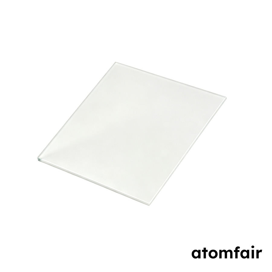
Magnesium Oxide (111) DSP Substrate 5×5×0.5 mm ATOMFAIR®
Price range: $66.99 through $207.99 -
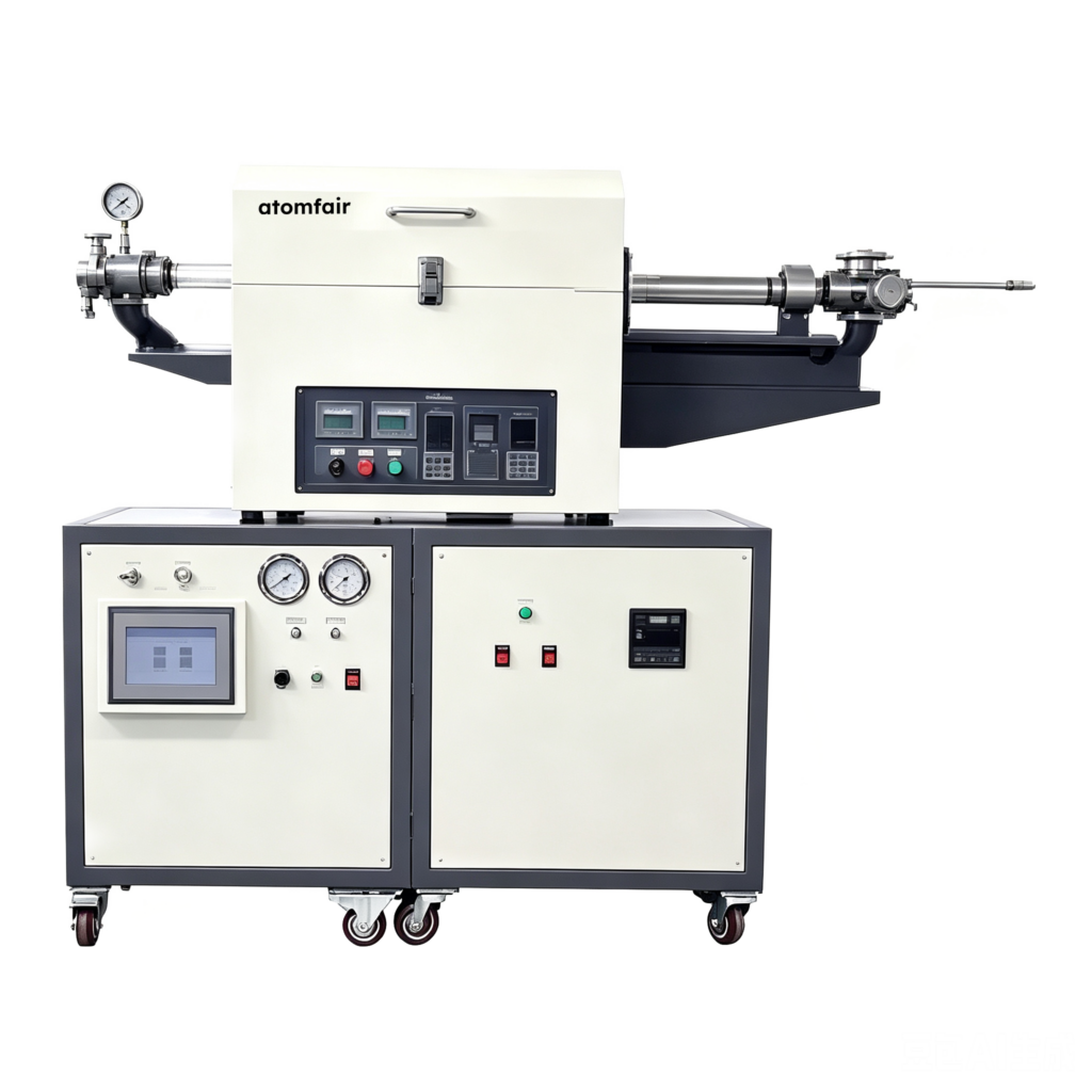
Magnetic Push-Pull 2D Materials System 1200°C
$6,500.00 -
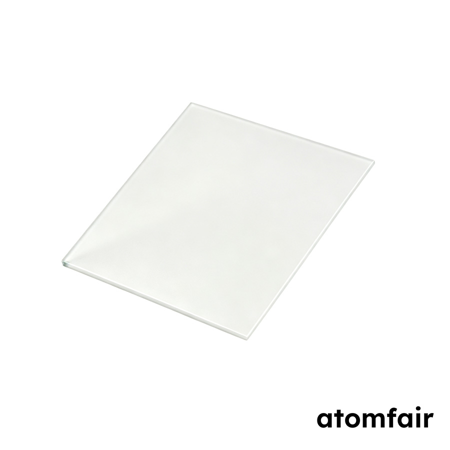
MgO Single Crystal Substrate (100) DSP 0.5mm ATOMFAIR®
Price range: $48.99 through $142.99 -
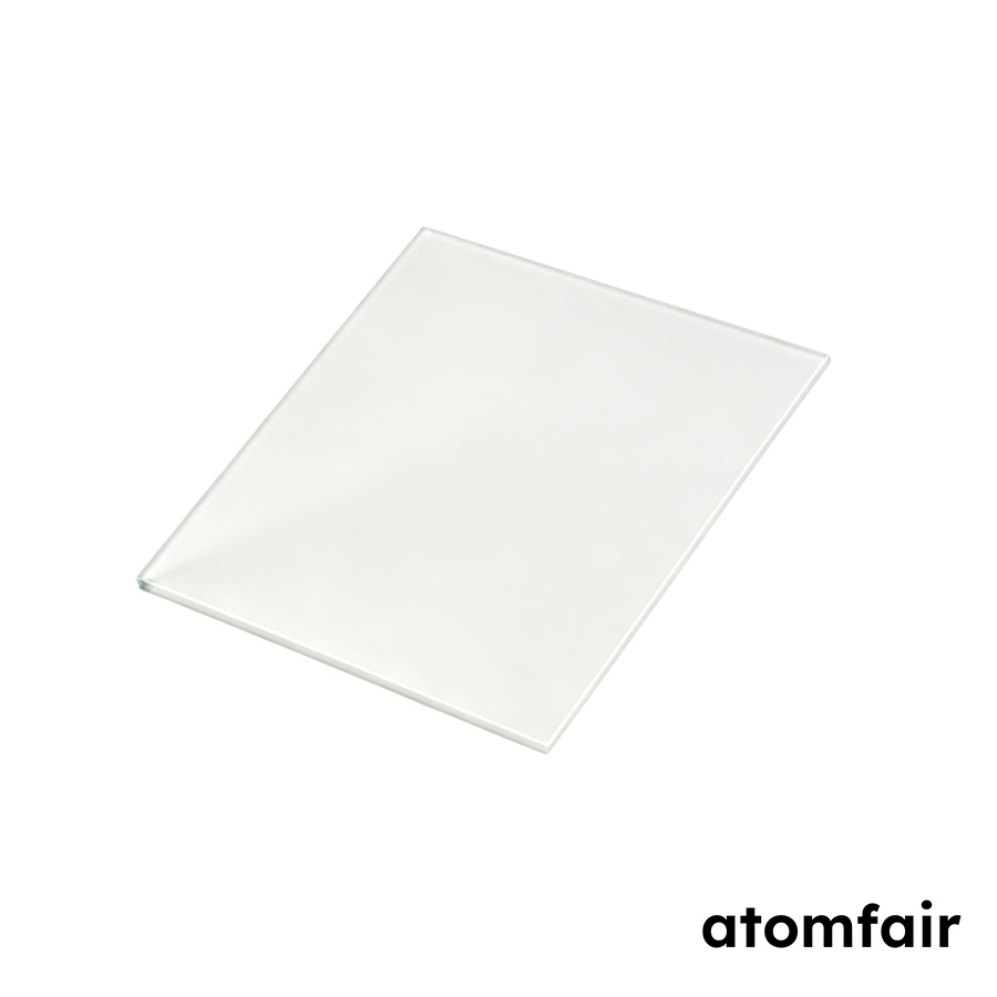
MgO Single Crystal Substrate (111) SSP 0.5 mm ATOMFAIR®
Price range: $52.99 through $317.99 -
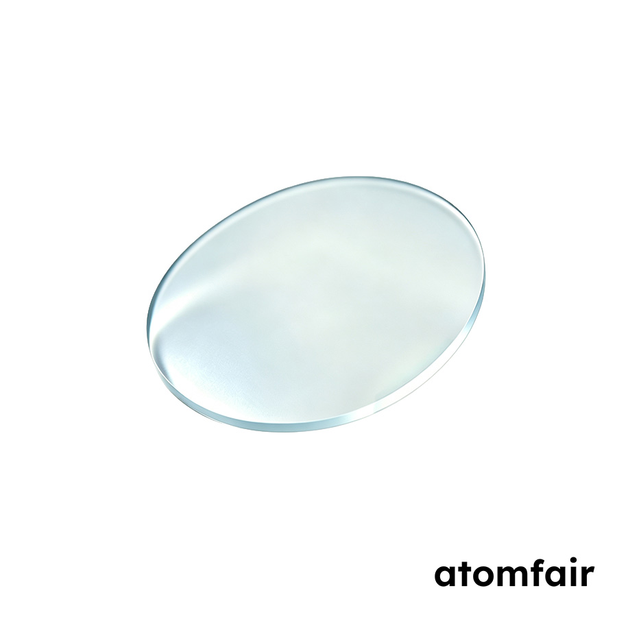
MgO Single Crystal Substrate Dia 8×0.5 mm ATOMFAIR®
$192.99 -
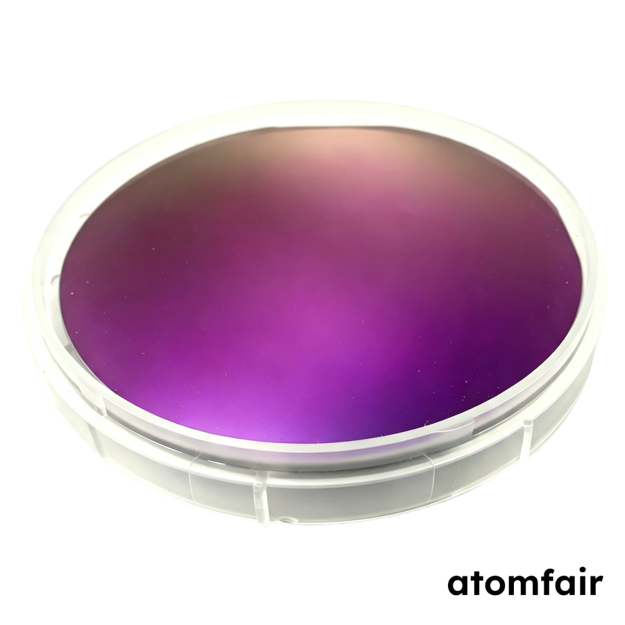
Monocrystalline Silicon Wafer 8 Inch 725±25μm ATOMFAIR®
$35.90 -
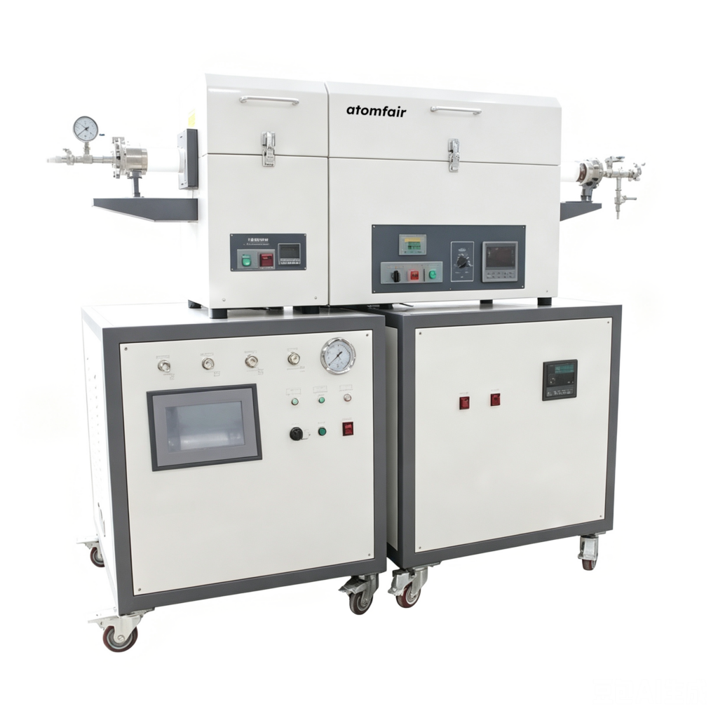
MoS2 Two-Dimensional CVD Preparation System 400°C
$6,500.00 -
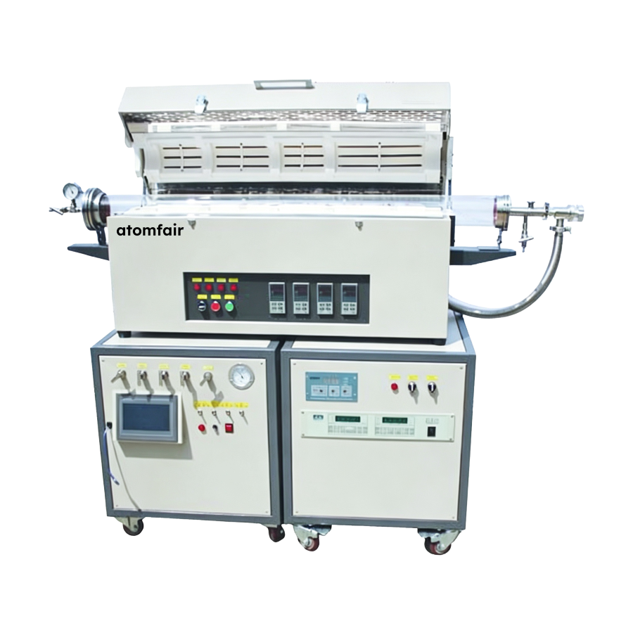
Multi-Zone CVD System 1200°C Thin-Film R&D ATOMFAIR®
$4,500.00 -
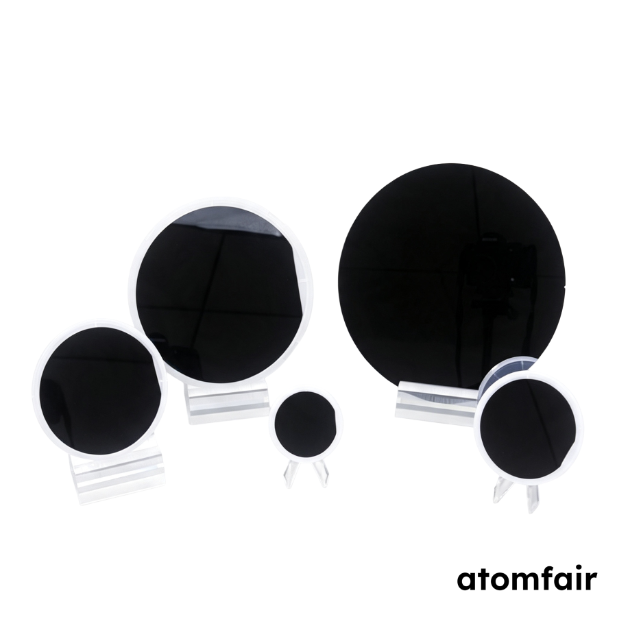
N-Type Silicon Wafer 2 in DSP 400μm ATOMFAIR®
$15.90 -
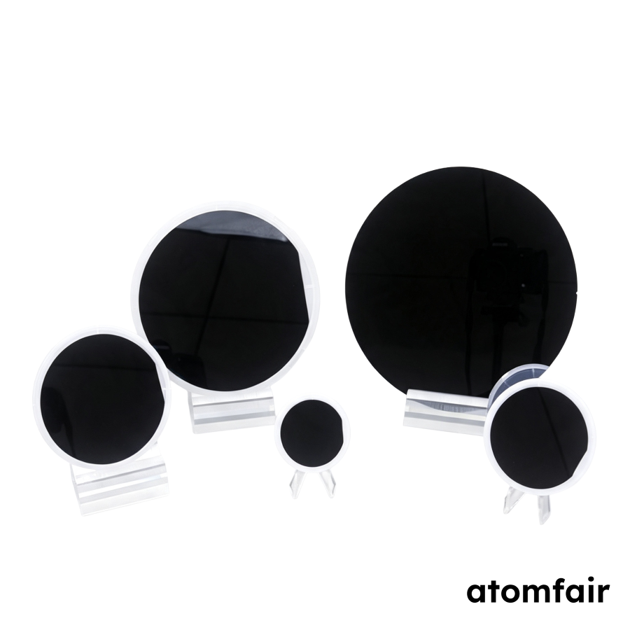
N-Type Silicon Wafer 2 in SSP 400 μm ATOMFAIR®
$19.90 -
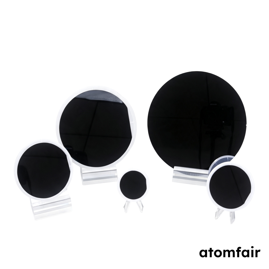
N-Type Silicon Wafer 2 inch 400μm SSP ATOMFAIR®
$15.90 -
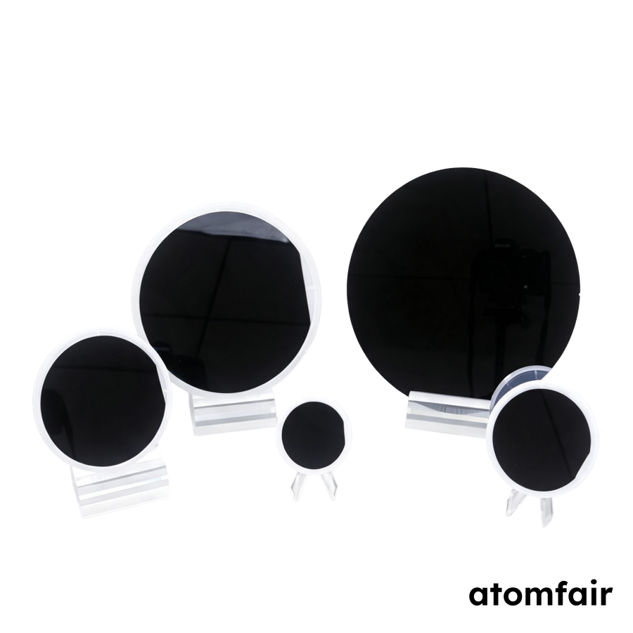
N-Type Silicon Wafer 4 in DSP 500μm ATOMFAIR®
$23.90 -
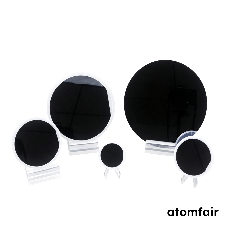
N-Type Silicon Wafer 6 in SSP 625μm ATOMFAIR®
$30.90 -
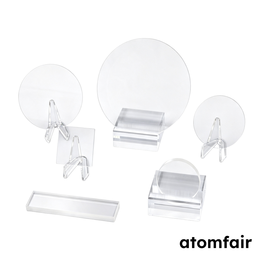
Off-Cut Sapphire Substrate 2 in 0.2° C/A SSP ATOMFAIR®
$32.90 -
Off-Cut Sapphire Substrate 2 in C/A 0.5° SSP ATOMFAIR®
$32.90 -
Off-Cut Sapphire Substrate 2 in C/A 1° SSP ATOMFAIR®
$32.90