|
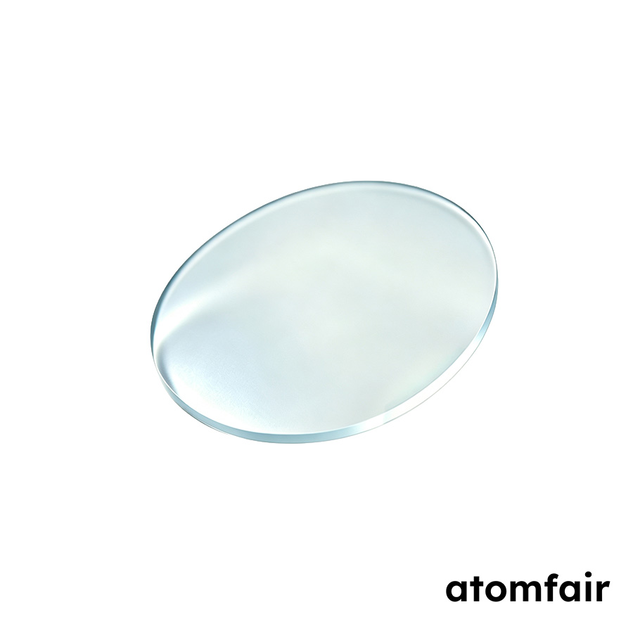
Magnesium Oxide Single Crystal Substrate, Dia. 8 × 0.5 mm, SSP, round wafer (10 pcs/box)
Product Type: MgO single crystal substrate
Research-grade laboratory product
|
|||||||||||||||||||||||||||||||||||||||
|
|||||||||||||||||||||||||||||||||||||||
|
LABORATORY PROCUREMENT SUPPORT
For model selection, accessory matching, platform compatibility or configuration confirmation, contact our technical sales team.
E-MAIL: inquiry@atomfair.com
|
|||||||||||||||||||||||||||||||||||||||
|
Manufacturer: Atomfair LLC
Brand: ATOMFAIR®
|
What optical and microwave properties does the Dia. 8 x 0.5 mm MgO single crystal substrate provide for thin-film research?
This MgO substrate is specified for optical transmission greater than 90% from 200 to 400 nm and greater than 98% from 500 to 1000 nm, with a dielectric constant of 9.8 and low dielectric constant and loss in the microwave band. These properties support ferroelectric, magnetic, optoelectronic, and high-temperature superconducting thin-film work as well as microwave filter research.
Can this one-side polished MgO wafer be used as an epitaxial substrate, and which lattice parameters are relevant for compatibility?
Yes, the substrate is intended for epitaxy and thin-film preparation. It has a cubic crystal structure with lattice constant a = 4.216 Å, a melting point of 2850°C, and a thermal expansion coefficient of 12.8 x 10^-6 /°C, which are the parameters to evaluate against the deposited film.
What specification and configuration details must be confirmed before ordering the Dia. 8 x 0.5 mm MgO substrate?
This listing is for a one-side polished (SSP), round wafer with dimensions Dia. 8 x 0.5 mm, supplied as 10 pieces per box. Before quotation, confirm Atomfair model AF-MgO-D8S, material, dimensions, orientation, thickness, and surface finish; custom orientation and size requests can also be confirmed for project-specific requirements.
This specific MgO single crystal substrate (Dia. 8 × 0.5 mm, SSP) offers high optical transmission (>90% UV, >98% visible-NIR) and low microwave dielectric loss, making it suitable for epitaxial thin-film research in optoelectronics and microwave filters, though its small size and single-side polish limit broader application.
Positive
- High optical transmission UV to NIR: Transmission >90% from 200-400 nm and >98% from 500-1000 nm enables sensitive optical characterization and photo-based thin-film deposition monitoring.
- Low microwave dielectric loss: Dielectric constant of 9.8 with low loss in the microwave band supports high-quality epitaxial growth for microwave filter and resonator research.
Trade-offs
- Single-side polished only: This listing specifies one-side polished (SSP) finish; double-side polished substrates require a separate purchase for applications needing both faces optically smooth.
- Small 8 mm diameter wafer: The 8 mm diameter limits sample area and may require specialized handling fixtures or adapters for processing equipment designed for larger standard wafer sizes.
Every advanced material, component, equipment, and instrument in our catalog is backed by rigorous testing. We maintain strict internal quality management frameworks and align with CE conformity metrics to deliver transparent, reproducible performance data via our public open-science repository.
To request raw batch performance data, submit formal vendor registration paperwork, or execute a fast-turnaround R&D manufacturing loop, contact us at inquiry@atomfair.com.
Item is dispatched under the Atomfair Shipping & Delivery Framework (Free worldwide shipping on orders over $59 USD excl. heavy equipment). Return is governed by the Atomfair Return & Refund Policy (7-day technical return window).