|
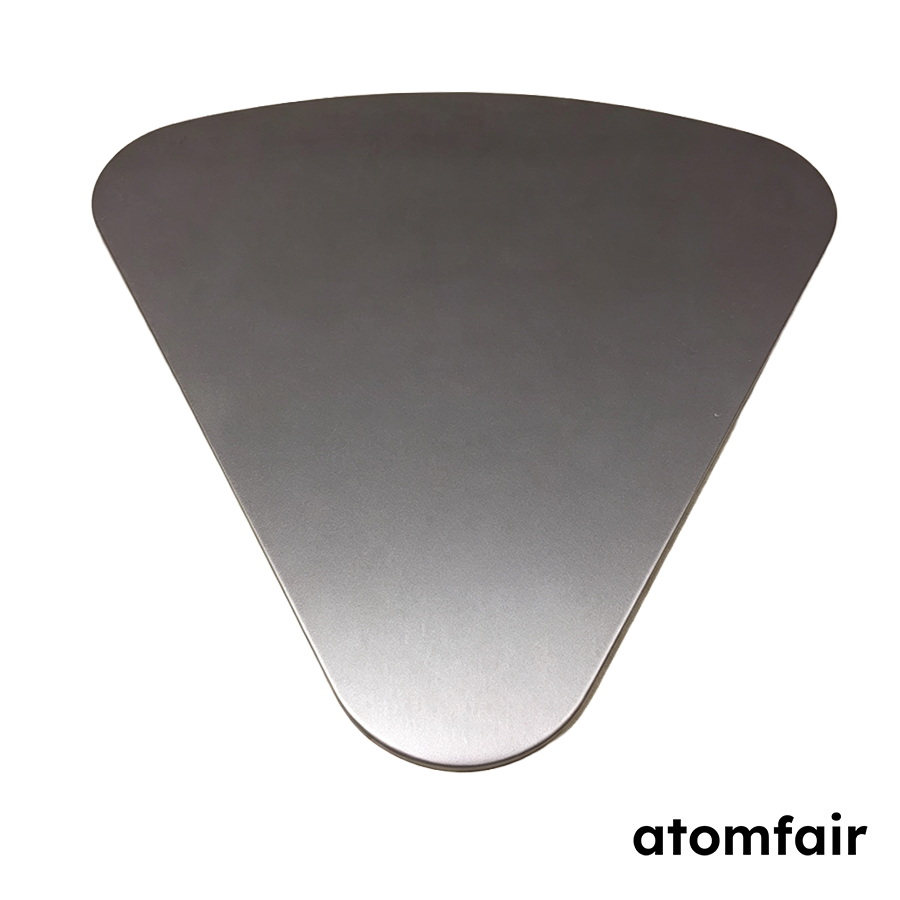
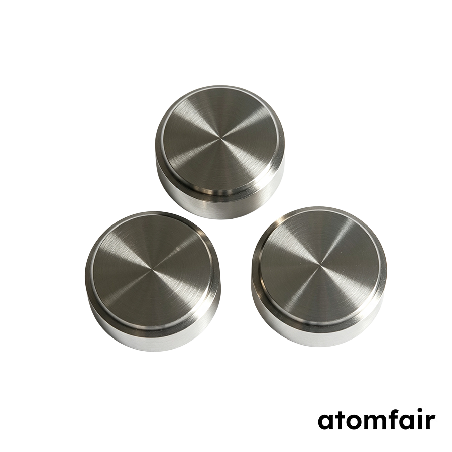
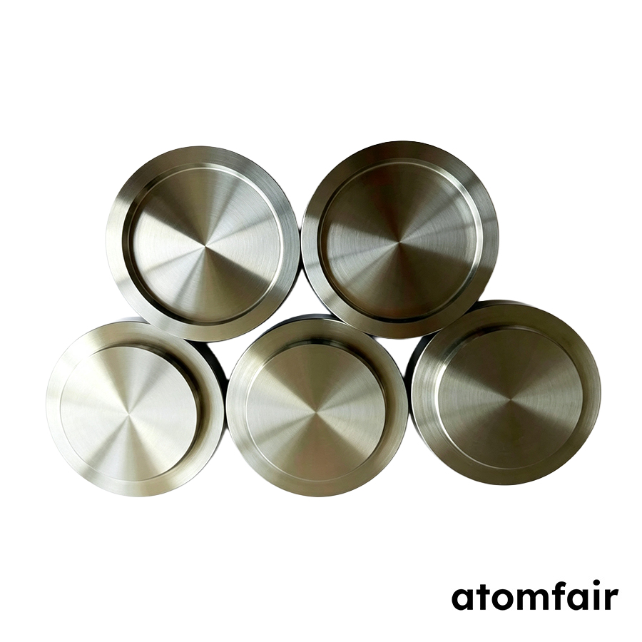
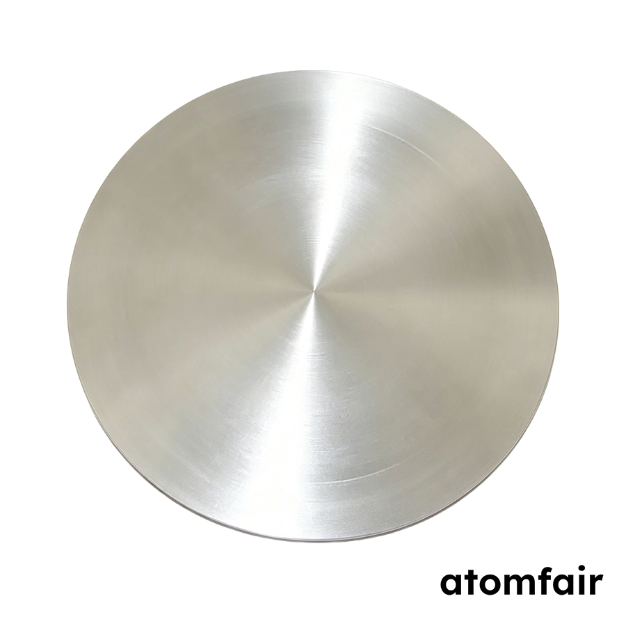
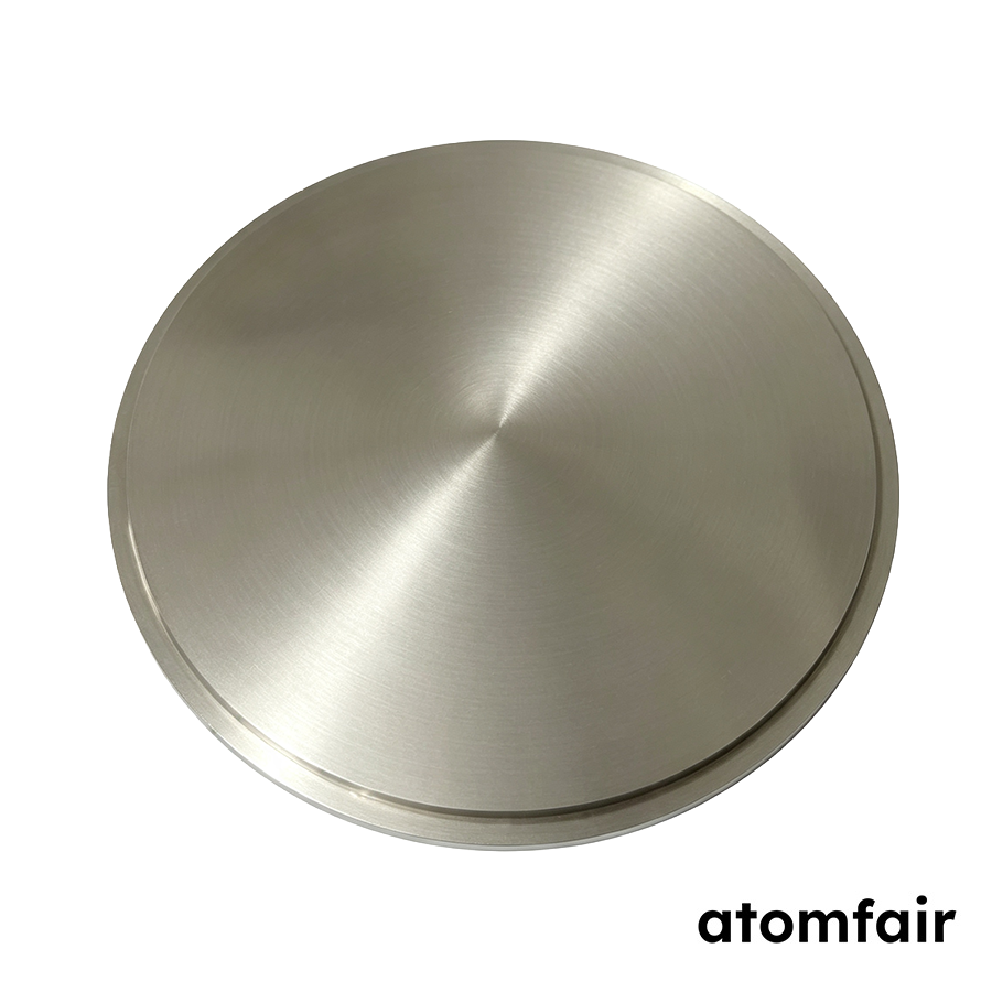
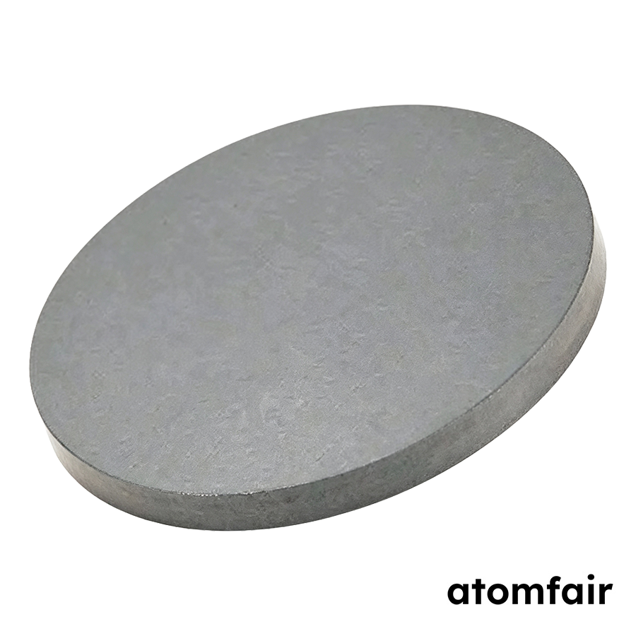
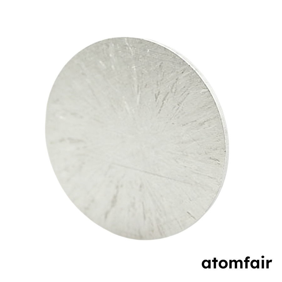
High Purity Antimony Sputtering Target, 99.99%
Product Type: Round planar sputtering target
Research-grade laboratory product
|
|||||||||||||||||||||||||||||||||||||
|
|||||||||||||||||||||||||||||||||||||
|
LABORATORY PROCUREMENT SUPPORT
For model selection, accessory matching, platform compatibility or configuration confirmation, contact our technical sales team.
INQUIRY: inquiry@atomfair.com
|
|||||||||||||||||||||||||||||||||||||
|
Manufacturer: Atomfair LLC
Brand: ATOMFAIR®
|
This document describes the configuration and handling constraints for the ATOMFAIR 99.99% antimony round planar sputtering target. It applies to the target itself across the listed thickness and diameter variations, supplied unbonded or with optional Cu backing plate bonding.
- Target surface preservation: Protect the turned/ground target surface from mechanical contact, scratching, or particulate contamination so that the typical Ra ≤ 1.6 μm finish is retained until mounting.
- Dimensional verification: Confirm the actual diameter and thickness against the ±0.10 mm tolerances and the receiving sputter source pocket dimensions before installation.
- Bonding selection: Specify whether the target is required unbonded or with Cu backing plate bonding before quotation, because the bonding option changes the delivered configuration.
- Delivery inspection and storage: Inspect the vacuum packaging and accompanying certificate of analysis on receipt, and keep the target sealed until the configuration is confirmed for installation.
What does the 99.99% purity and 39.0 micro-ohm cm resistivity of this antimony sputtering target mean for thin-film deposition?
This target is specified at 99.99% purity (material grade Sb 3N5) with typical total critical impurities <=100 ppm, a density of 6.70 g/cm³, and electrical resistivity of 39.0 micro-ohm cm. These parameters support controlled sputtering behavior for semiconductor/thermoelectric film, alloy films, and magnetron sputtering. Final film properties still depend on deposition parameters and system configuration.
Which diameter and thickness options are available for this round planar antimony target, and what tolerances apply?
This round planar sputtering target is offered in thicknesses of 3, 4, 5, 6, and 6.35 mm and diameters of 25.4, 50, 50.8, 60, 76.2, 80.0, 101.6, and 100 mm. Typical dimensional tolerances are diameter +/-0.10 mm and thickness +/-0.10 mm. Confirm the exact dimensions against your sputter source before quotation because the target is manufactured to the agreed configuration.
Is this antimony sputtering target supplied bonded or unbonded, and what surface condition should I expect?
The target is supplied unbonded, with an optional Cu backing plate bonding option available if your system requires a bonded configuration. The surface finish is turning/grinding with Ra<=1.6 μm (typical). It is vacuum packed with a COA, and final parameters are confirmed by batch inspection and the agreed configuration.
The 99.99% pure antimony sputtering target (AF-MT-S-ANTI-N40X-ORMF) offers a round planar geometry with controlled surface finish (Ra ≤ 1.6 µm) and tight dimensional tolerances (±0.10 mm), suitable for semiconductor/thermoelectric film and magnetron sputtering applications, though unbonded delivery requires separate backing plate integration.
Positive
- High purity with low critical impurities: 99.99% purity grade with typical total critical impurities ≤100 ppm ensures controlled deposition chemistry for sensitive semiconductor and thermoelectric film workflows.
- Broad dimensional configurability: Available in 8 diameters (25.4–101.6 mm) and 5 thicknesses (3–6.35 mm) allows matching to diverse magnetron sputtering cathode geometries without custom fabrication.
Trade-offs
- Unbonded delivery requires integration: Supplied unbonded by default; optional backing plate bonding must be specified at quotation, adding a procurement step for systems requiring bonded targets.
- Surface finish variability per batch: Surface roughness Ra ≤ 1.6 µm is typical but confirmed by batch inspection, meaning final surface condition may vary slightly between production lots.
Every advanced material, component, equipment, and instrument in our catalog is backed by rigorous testing. We maintain strict internal quality management frameworks and align with CE conformity metrics to deliver transparent, reproducible performance data via our public open-science repository.
To request raw batch performance data, submit formal vendor registration paperwork, or execute a fast-turnaround R&D manufacturing loop, contact us at inquiry@atomfair.com.
Item is dispatched under the Atomfair Shipping & Delivery Framework (Free worldwide shipping on orders over $59 USD excl. heavy equipment). Return is governed by the Atomfair Return & Refund Policy (7-day technical return window).