|
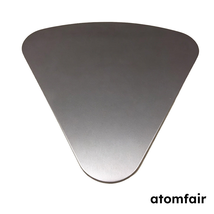
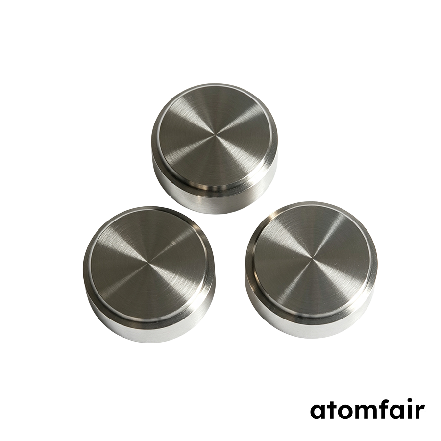
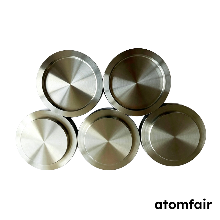
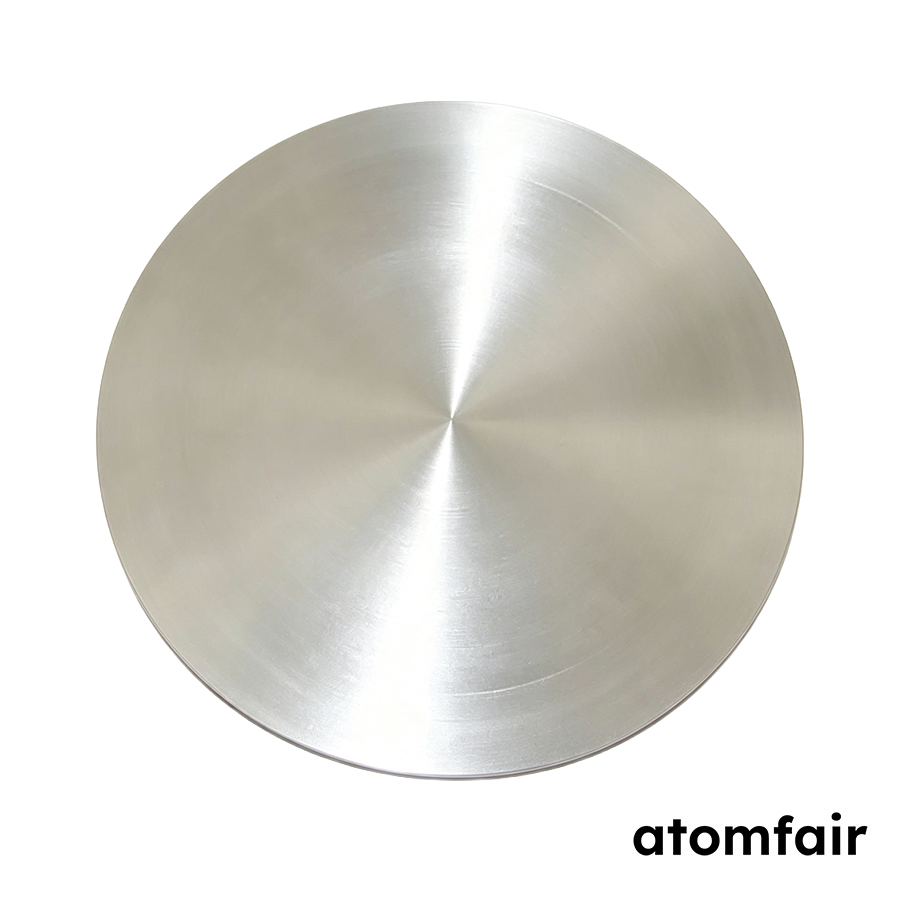
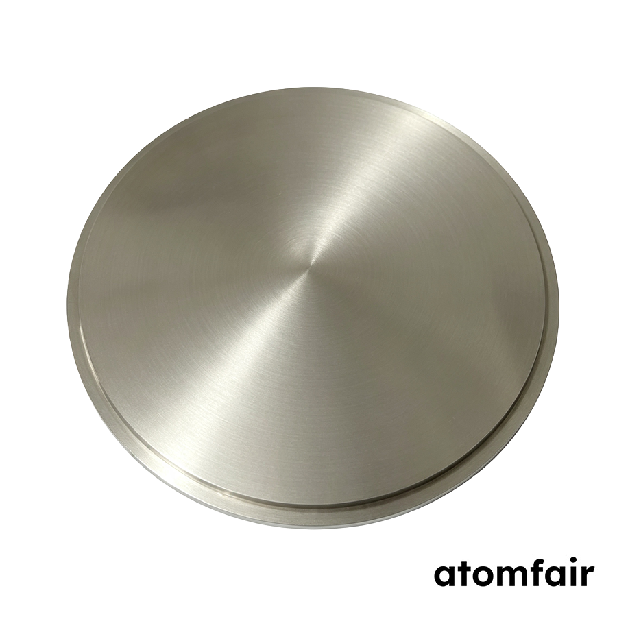
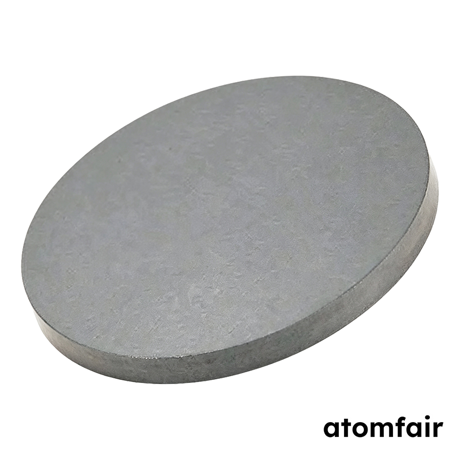
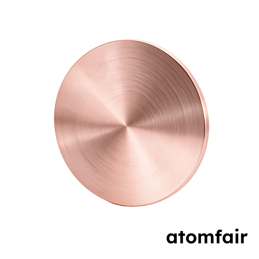
High Purity Copper Sputtering Target, 99.995%
Product Type: Round planar sputtering target
Research-grade laboratory product
|
|||||||||||||||||||||||||||||||||||||
|
|||||||||||||||||||||||||||||||||||||
|
LABORATORY PROCUREMENT SUPPORT
For model selection, accessory matching, platform compatibility or configuration confirmation, contact our technical sales team.
INQUIRY: inquiry@atomfair.com
|
|||||||||||||||||||||||||||||||||||||
|
Manufacturer: Atomfair LLC
Brand: ATOMFAIR®
|
Handling must preserve the machined target face and the sealed delivery state until the target is mounted. Confirmation of the bonding configuration and dimensional fit is required before installation.
- Surface integrity preservation: Avoid touching or abrading the prepared target face to prevent surface damage that could affect sputtering behavior.
- Bonding configuration confirmation: Confirm before installation whether the target will be used unbonded or bonded to a Cu backing plate.
- Dimensional fit verification: Verify that the selected diameter and thickness are compatible with the sputter source before mounting.
- Seal retention: Keep the target in its protective delivery packaging until immediately before mounting to limit exposure to handling contamination.
What effect do the 99.995% purity and 1.68 micro-ohm cm resistivity of this copper sputtering target have on deposited conductive films?
This Cu 4N5 round planar target is specified at 99.995% purity with typical total critical impurities <=50 ppm, which supports controlled sputtering workflows for conductive films and interconnect layers. Its electrical resistivity is 1.68 micro-ohm cm and density is 8.96 g/cm^3, so the material is specified for magnetron sputtering of electronic-device metallization rather than a general-purpose commodity copper source.
Which thickness and diameter configurations are available for this round planar copper target, and what tolerances should be checked for sputter tool compatibility?
Available thicknesses are 3 mm, 4 mm, 5 mm, 6 mm and 6.35 mm, and available diameters are 25.4 mm, 50 mm, 50.8 mm, 60 mm, 76.2 mm, 80.0 mm, 101.6 mm and 100 mm. The typical dimensional tolerance is diameter +/-0.10 mm and thickness +/-0.10 mm, so you should confirm the target holder working range, required configuration and consumables before quotation, as the final parameters are confirmed by batch inspection and the agreed configuration.
Does this copper sputtering target ship unbonded, and what should be confirmed before mounting it in a sputtering system?
The target is supplied unbonded, with optional Cu backing plate bonding available as a configuration choice. Because the selected bonding option changes the physical configuration supplied, confirm the unbonded or bonded option, model, working range and compatibility with your system before quotation; the target is vacuum packed with a certificate of analysis and final parameters are batch-inspected.
Atomfair AF-CU-99N995 round planar copper sputtering target provides 99.995% purity, 8.96 g/cm3 density, and 1.68 micro-ohm cm electrical resistivity for conductive film and interconnect deposition, with multiple diameter and thickness options. Buyers must confirm the unbonded/backing-plate configuration and typical batch-inspected dimensional tolerances before quotation.
Positive
- 4N5 purity with low critical impurities: Cu 4N5 grade with 99.995% purity and typical total critical impurities <=50 ppm supports controlled sputtering workflows for conductive films, interconnect layers, and electronic device metallization.
- Low resistivity for sputter deposition: The 1.68 micro-ohm cm electrical resistivity and 8.96 g/cm3 density are consistent with magnetron sputtering requirements for conductive thin-film applications.
Trade-offs
- Unbonded by default; backing plate optional: The target is supplied unbonded, and copper backing plate bonding is only available as an optional configuration. Users must specify and confirm this requirement before quotation if their sputtering source needs a backing plate.
- Typical tolerances require configuration confirmation: Diameter and thickness tolerances are +/-0.10 mm typical and surface roughness is Ra<=1.6 um typical. Final parameters are confirmed by batch inspection against the agreed configuration, so procurement must verify the exact dimensional and surface requirements beforehand.
Every advanced material, component, equipment, and instrument in our catalog is backed by rigorous testing. We maintain strict internal quality management frameworks and align with CE conformity metrics to deliver transparent, reproducible performance data via our public open-science repository.
To request raw batch performance data, submit formal vendor registration paperwork, or execute a fast-turnaround R&D manufacturing loop, contact us at inquiry@atomfair.com.
Item is dispatched under the Atomfair Shipping & Delivery Framework (Free worldwide shipping on orders over $59 USD excl. heavy equipment). Return is governed by the Atomfair Return & Refund Policy (7-day technical return window).