|
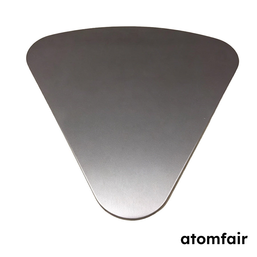
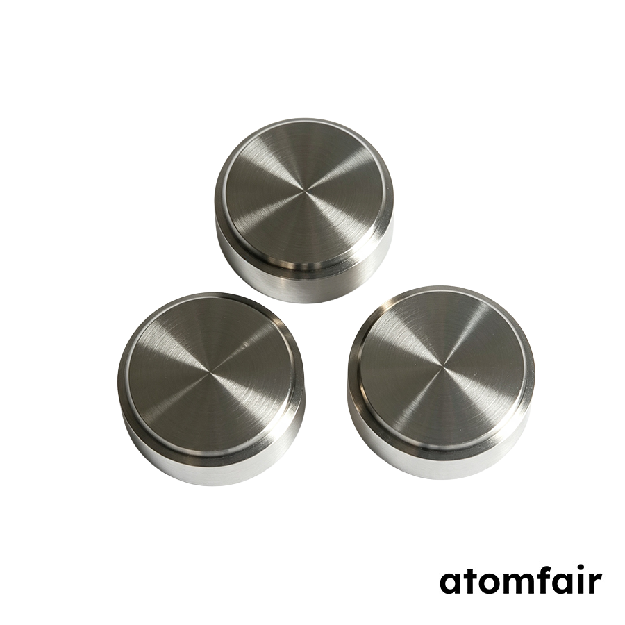
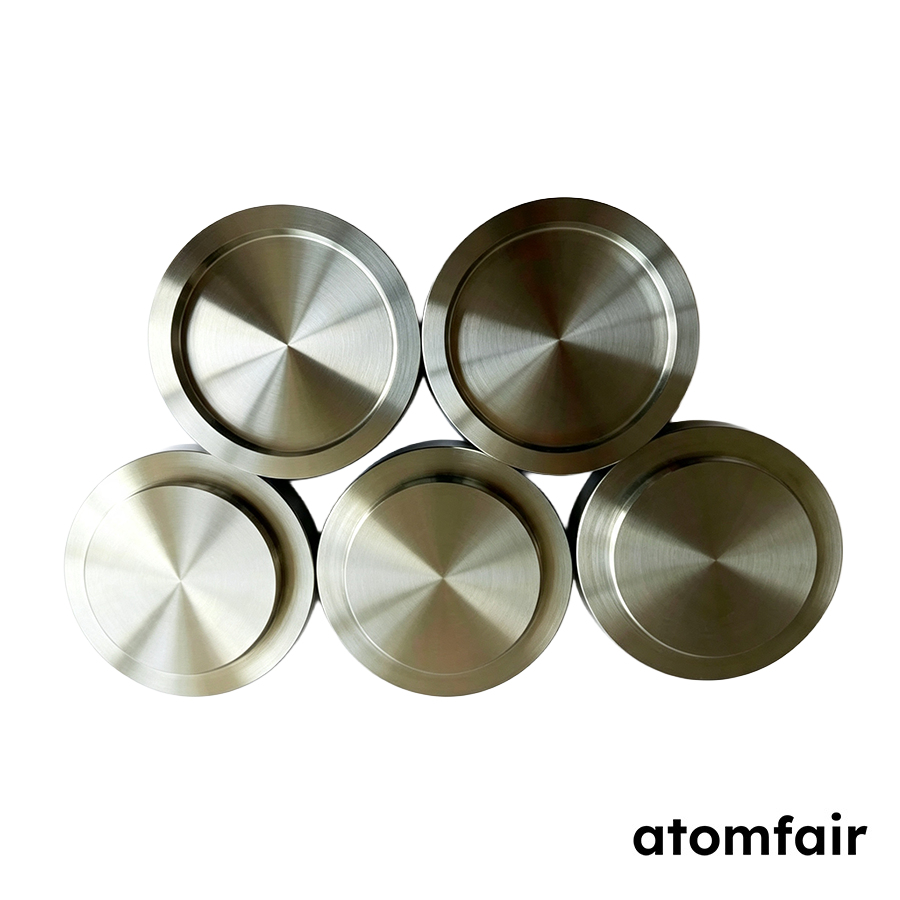
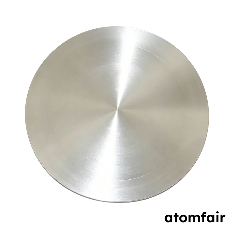
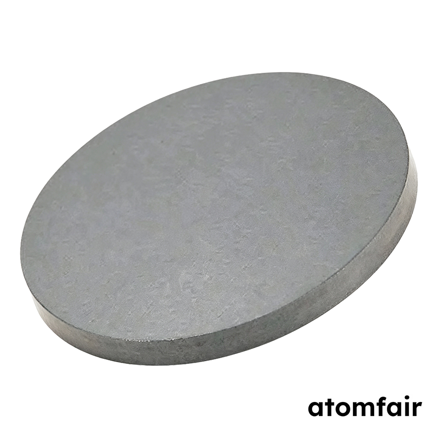
Tungsten-Tantalum Alloy Sputtering Target (WTa)
Product Type: Metal alloy sputtering target
Research-grade laboratory product
|
|||||||||||||||||||||||||||||||||||||
|
|||||||||||||||||||||||||||||||||||||
|
LABORATORY PROCUREMENT SUPPORT
INQUIRY: inquiry@atomfair.com
|
|||||||||||||||||||||||||||||||||||||
|
Manufacturer: Atomfair LLC
Brand: ATOMFAIR®
|
Store the target in a dry, inert atmosphere to prevent surface oxidation and contamination. Avoid exposure to moisture or reactive gases that may degrade the sputtering surface.
- Environmental Sensitivity: The target must be stored in a vacuum or inert gas environment to maintain surface purity and prevent oxidation prior to deposition.
- Handling Constraint: Handle the target using clean, powder-free gloves to avoid transferring oils or particulates that could compromise film adhesion.
- Bonding Constraint: Select indium or elastomer bonding based on the maximum power density and thermal load of the intended sputtering process to avoid bond failure.
- Substrate Preparation Requirement: Properly prepare substrates to achieve adhesion strength greater than 15 MPa as specified by ASTM D4541 pull-off testing.
Mount the target into the magnetron cathode using the appropriate bonding method and backing plate. Condition the target surface by pre-sputtering to remove any native oxide layer before deposition.
Required Equipment: Magnetron sputtering system with DC or RF power supply, Vacuum chamber capable of 0.5-2.0 Pa Ar atmosphere, Clean, powder-free gloves
- Inspect target and bonding interface
Inspect the target surface and bonding layer for any visible defects, cracks, or contamination before mounting. - Mount target onto backing plate
Mount the target onto the selected backing plate using the specified bonding method, ensuring full thermal contact. - Install assembly into sputtering cathode
Install the bonded target assembly into the magnetron cathode, tightening all fasteners to the manufacturer's torque specification. - Evacuate chamber and introduce argon
Evacuate the deposition chamber to base pressure below 1e-4 Pa, then backfill with argon to the operating pressure range of 0.5-2.0 Pa. - Pre-sputter to remove surface oxide
Pre-sputter the target for 5-10 minutes at low power density (3-5 W/cm² DC or 1-2 W/cm² RF) with shutter closed to remove any native oxide layer. - Set deposition parameters and begin coating
Set the desired power density within the specified range (3-15 W/cm² DC or 1-5 W/cm² RF) and open the shutter to begin deposition on the substrate.
What power density and deposition rate ranges are recommended for the WTa alloy sputtering target in DC and RF magnetron sputtering?
For DC magnetron sputtering, the recommended power density range is 3–15 W/cm², and for RF it is 1–5 W/cm², under an Ar atmosphere of 0.5–2.0 Pa. Under these conditions, deposition rates of 10–80 nm/min with ±5% thickness uniformity across a 100 mm substrate can be achieved.
What bonding and backing plate configurations are available for the WTa target, and how do they influence thermal management and system compatibility?
The WTa target is available with optional indium bonding or elastomer bonding, and the backing plate can be oxygen-free copper or CuCrZr. These options affect heat dissipation and mounting compatibility with different sputtering systems, so buyers should confirm bonding and backing plate requirements against their deposition setup.
What adhesion strength and film properties can be expected from WTa deposited films under optimized conditions?
Deposited WTa films exhibit adhesion strength greater than 15 MPa (ASTM D4541 pull-off test) on properly prepared substrates. The films are suitable for applications such as diffusion barriers, gate electrodes, and high-temperature protective coatings due to the combination of the WTa composition and 99.95% purity with total metallic impurities below 500 ppm and O+N below 100 ppm.
The WTa sputtering target offers 99.95% purity with <500 ppm metallic impurities and <100 ppm O+N, enabling stoichiometric film deposition with ±5% thickness uniformity over 100 mm substrates. However, its operational constraints require precise DC/RF sputtering parameters (3-15 W/cm² DC, 1-5 W/cm² RF, 0.5-2.0 Pa Ar) and careful selection of bonding and backing plate options for integration into existing deposition systems.
Positive
- High purity and low contamination: 99.95% (3N5) purity with total metallic impurities <500 ppm and O+N <100 ppm minimizes contamination, improving deposited film resistivity and adhesion.
- Optimized deposition uniformity: DC/RF magnetron sputtering at 3-15 W/cm² (DC) or 1-5 W/cm² (RF) under 0.5-2.0 Pa Ar yields deposition rates of 10-80 nm/min with ±5% thickness uniformity across a 100 mm substrate.
Trade-offs
- Strict sputtering parameter requirements: Target is optimized for DC/RF magnetron sputtering within narrow power density (3-15 W/cm² DC, 1-5 W/cm² RF) and Ar pressure (0.5-2.0 Pa) ranges; deviations may affect deposition rate and film quality.
- Optional bonding and backing plate: Bonding type (indium/elastomer) and backing plate (oxygen-free copper/CuCrZr) are optional; improper selection or mismatch with deposition system can cause thermal or adhesion issues, requiring careful procurement verification.
Every advanced material, component, equipment, and instrument in our catalog is backed by rigorous testing. We maintain strict internal quality management frameworks and align with CE conformity metrics to deliver transparent, reproducible performance data via our public open-science repository.
To request raw batch performance data, submit formal vendor registration paperwork, or execute a fast-turnaround R&D manufacturing loop, contact us at inquiry@atomfair.com.
Item is dispatched under the Atomfair Shipping & Delivery Framework (Free worldwide shipping on orders over $59 USD excl. heavy equipment). Return is governed by the Atomfair Return & Refund Policy (7-day technical return window).