|
Cobalt-Iron-Silicon Alloy Sputtering Target (CoFeSi)
Product Type: Metal alloy sputtering target
Research-grade laboratory product
|
|||||||||||||||||||||||||||||||||||||
|
|||||||||||||||||||||||||||||||||||||
|
LABORATORY PROCUREMENT SUPPORT
INQUIRY: inquiry@atomfair.com
|
|||||||||||||||||||||||||||||||||||||
|
Manufacturer: Atomfair LLC
Brand: ATOMFAIR®
|
This sputtering target requires controlled vacuum deposition conditions with DC/RF magnetron sputtering at specified power densities and argon pressure to achieve stoichiometric film transfer. The target must be bonded to an appropriate backing plate and handled in a clean environment to prevent contamination and ensure adhesion strength above 15 MPa.
- Power Density Constraint: Operate DC sputtering at 3-15 W/cm² or RF sputtering at 1-5 W/cm² to avoid target damage and maintain deposition rate.
- Atmosphere Constraint: Maintain argon pressure between 0.5-2.0 Pa during sputtering to achieve optimal plasma conditions and film uniformity.
- Bonding Requirement: Select indium or elastomer bonding as needed for thermal management and mechanical stability during deposition.
- Substrate Preparation: Prepare substrates to achieve adhesion strength greater than 15 MPa per ASTM D4541 pull-off test.
- Contamination Control: Ensure total metallic impurities below 500 ppm and O+N below 100 ppm to minimize film contamination.
What are the optimal DC and RF magnetron sputtering conditions for the CoFeSi alloy target to achieve high deposition rate and uniform film thickness?
For DC sputtering, optimal power density is 3–15 W/cm², and for RF sputtering 1–5 W/cm², under 0.5–2.0 Pa Ar atmosphere, achieving deposition rates of 10–80 nm/min with ±5% thickness uniformity across a 100 mm substrate. Fine-tuning within these ranges depends on target age and substrate temperature, but the stated conditions yield consistent stoichiometric transfer within ±2 at%.
Which bonding type and backing plate material should be selected for the CoFeSi target when used in a high-power sputtering system?
The CoFeSi target is available with optional indium bonding or elastomer bonding, and backing plates in oxygen-free copper or CuCrZr. Indium bonding provides superior thermal conductivity for high-power DC sputtering up to 15 W/cm², while elastomer bonding is better suited for RF applications or lower power densities to avoid thermal stress. The choice depends on your system’s cooling and power profile.
How does the fine grain size (≤50 µm) of the CoFeSi target influence film quality and target erosion uniformity?
The fine-grained structure ensures homogeneous sputtering erosion, reducing arcing and particle generation. With ≥95% relative density and Ra ≤0.8 µm surface finish, the target minimizes nodule formation, extending usable life and maintaining consistent deposition rates over multiple runs.
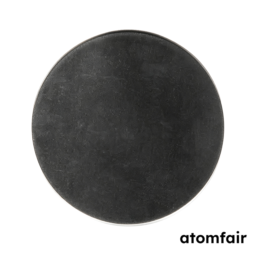
The CoFeSi alloy sputtering target (99.95% purity, 2 in diameter × 0.125 in) is evaluated for DC/RF magnetron sputtering, offering stoichiometric film transfer within ±2 at% and deposition rates of 10–80 nm/min with ±5% thickness uniformity on 100 mm substrates, but requires careful power density management and bonding selection to avoid thermal stress or target cracking.
Positive
- High purity with low metallic impurities: 99.95% (3N5) purity with total metallic impurities <500 ppm and O+N <100 ppm minimizes contamination, improving deposited film resistivity and adhesion for magnetic recording and biomedical coatings.
- Fine-grained microstructure for uniform sputtering: Grain size ≤50 µm and relative density ≥95% of theoretical ensure consistent erosion and film thickness uniformity of ±5% across a 100 mm substrate under optimized conditions.
Trade-offs
- Narrow power density operating window: DC sputtering requires 3–15 W/cm² and RF 1–5 W/cm²; exceeding these limits risks target cracking or thermal degradation, demanding precise power control and system calibration.
- Bonding and backing plate dependency: Indium or elastomer bonding and oxygen-free copper or CuCrZr backing plates are optional but must be matched to the deposition system's thermal and mechanical constraints to prevent delamination or warping during sputtering.
Every advanced material, component, equipment, and instrument in our catalog is backed by rigorous testing. We maintain strict internal quality management frameworks and align with CE conformity metrics to deliver transparent, reproducible performance data via our public open-science repository.
To request raw batch performance data, submit formal vendor registration paperwork, or execute a fast-turnaround R&D manufacturing loop, contact us at inquiry@atomfair.com.
Item is dispatched under the Atomfair Shipping & Delivery Framework (Free worldwide shipping on orders over $59 USD excl. heavy equipment). Return is governed by the Atomfair Return & Refund Policy (7-day technical return window).