
Deposition & Thin-Film Materials
Deposition & Thin-Film Materials supports vacuum coating, thin-film preparation, materials research, and functional coating development. The range covers evaporation materials, sputtering targets, and materials used in thin-film deposition for electronics, semiconductors, optics, displays, energy devices, magnetic materials, sensors, protective coatings, and advanced materials research.
Materials can be selected by deposition method, material system, film function, purity, physical form, dimensions, and process compatibility. Whether developing conductive films, optical coatings, magnetic layers, dielectric films, wear-resistant coatings, diffusion barriers, or new thin-film processes, customers can begin by selecting the appropriate material family.
When making an inquiry, please provide the required material or formula, purity, material form or target dimensions, deposition method, quantity, substrate type, and any technical documentation requirements.
Show More: Select by Deposition Method, Material System, and Film Requirement
Main Material Types
| Material Type | Typical Material Range | Typical Applications | Selection Considerations |
|---|---|---|---|
| Pure Metal Evaporation Materials | Aluminum, copper, silver, gold, chromium, titanium, nickel, molybdenum, tungsten, platinum, and other metals | Conductive layers, electrodes, reflective films, adhesion layers, and functional metal films | Element, purity, physical form, and evaporation-source compatibility |
| Alloy Evaporation Materials | Aluminum alloys, nickel alloys, titanium alloys, magnetic alloys, precious-metal alloys, and functional alloys | Alloy films, magnetic films, barrier layers, and specialized functional coatings | Nominal composition, evaporation behavior, and required film performance |
| Oxide Evaporation Materials | Metal oxides, transparent conductive oxides, dielectric oxides, and functional oxides | Optical films, transparent conductive films, insulating layers, sensors, and functional thin films | Chemical composition, thermal stability, and film-function requirements |
| Nitride Evaporation Materials | Metal nitrides and functional nitride compounds | Hard coatings, wear-resistant layers, diffusion barriers, electronic films, and optical films | Material system, process temperature, hardness, and film stability |
| Carbide Evaporation Materials | Metal carbides and high-temperature compounds | Wear-resistant coatings, high-temperature films, and hard functional layers | Melting behavior, evaporation method, and required film density |
| Chalcogenide Evaporation Materials | Sulfides, selenides, tellurides, and related compounds | Optoelectronic materials, infrared materials, thin-film solar research, and semiconductor studies | Stoichiometry, purity, and thermal stability |
| Halide Evaporation Materials | Fluorides, chlorides, bromides, iodides, and related materials | Optical coatings, infrared-transmitting films, and electron-beam evaporation processes | Optical properties, deposition conditions, and film purpose |
| Phosphide and Antimonide Evaporation Materials | Metal phosphides, antimonides, and related compounds | Compound semiconductors, optoelectronic devices, and functional thin-film research | Chemical composition, intended film application, and process compatibility |
| Specialty Compound Evaporation Materials | Complex oxides, borides, silicides, chalcogenides, and other functional compounds | Specialized optical, electronic, magnetic, and advanced functional films | Performance target, deposition method, and project requirements |
| Sputtering Targets | Pure metal targets, alloy targets, oxide targets, ceramic targets, and compound targets | DC sputtering, RF sputtering, magnetron sputtering, and thin-film preparation | Composition, dimensions, thickness, purity, and equipment configuration |
| CVD / ALD Precursor Materials | Metal-organic precursors, halide precursors, silicon sources, and other vapor-deposition materials | Chemical vapor deposition, atomic layer deposition, semiconductor processing, and highly uniform thin films | Precursor chemistry, process temperature, reaction system, and equipment compatibility |
Select by Film Function
| Film Requirement | Material Directions to Consider |
|---|---|
| Conductive Layers and Electrodes | Pure metals, precious metals, copper-based, aluminum-based, nickel-based, and transparent conductive oxide materials |
| Optical and Antireflection Films | Oxides, fluorides, sulfides, and other optical functional compounds |
| Semiconductor and Electronic Films | High-purity metals, silicides, phosphides, antimonides, oxides, and CVD / ALD precursors |
| Magnetic and Sensor Films | Iron-based, cobalt-based, nickel-based, rare-earth, and other functional alloy materials |
| Wear-Resistant, Corrosion-Resistant, and Protective Films | Nitrides, carbides, oxides, refractory metals, and alloy materials |
| Barrier and Interface Layers | Titanium, chromium, molybdenum, tungsten, tantalum, nickel-based, and related alloy or compound materials |
| Energy and Functional Device Films | Oxides, chalcogenides, phosphides, specialty compounds, and composite materials |
Information to Confirm Before Ordering
| Information | Why It Matters |
|---|---|
| Deposition Method | Matches the material to evaporation, sputtering, CVD, ALD, or another thin-film process. |
| Material Composition | Defines the chemical system and intended film function. |
| Purity Requirement | Supports impurity-control requirements for electronic, optical, semiconductor, or general research applications. |
| Material Form | Evaporation materials may be selected as pellets, granules, pieces, sheets, wire, or other forms; sputtering targets require compatible dimensions and geometry. |
| Film Requirement | Helps identify suitable materials for conductive, insulating, magnetic, optical, protective, or other functional layers. |
| Equipment Conditions | Confirms compatibility with the evaporation source, crucible, electron-beam system, target holder, power mode, and vacuum system. |
| Substrate and Process Conditions | Supports selection based on substrate material, temperature, atmosphere, film thickness, and post-treatment requirements. |
Frequently Asked Questions
What is the difference between evaporation materials and sputtering targets?
Evaporation materials are vaporized in vacuum by heating or electron-beam methods and deposited onto a substrate. Sputtering targets are solid source materials used in plasma-assisted deposition. The suitable choice depends on the deposition equipment and process route.
How should I choose a thin-film material?
Start with the required film function, such as conductivity, insulation, reflectivity, optical transmission, hardness, magnetic response, or barrier performance. Then confirm the deposition method, substrate, process temperature, purity requirement, and equipment conditions.
Is higher purity always better?
Not every application requires the same purity level. Higher-purity materials are often preferred for impurity-sensitive electronic, optical, and semiconductor applications, while other thin-film projects should select purity according to practical performance and process requirements.
What forms are commonly available for evaporation materials?
Common forms include pellets, granules, pieces, sheets, powder, wire, rods, and custom shapes. The appropriate form depends on the evaporation source design, loading method, and material-utilization requirements.
What should be considered when selecting a sputtering target?
Confirm the material composition, purity, target diameter or rectangular dimensions, thickness, target shape, power mode, and deposition-system configuration. Backing plates, bonding, and specialized dimensions should also be considered where applicable.
What are oxide, nitride, and carbide materials typically used for?
Oxides are commonly used in optical, dielectric, transparent conductive, and functional films. Nitrides are often selected for hard, wear-resistant, and barrier coatings. Carbides are generally considered for high-temperature, high-hardness, and wear-resistant film applications.
Can these materials be used for research and small-batch process development?
Yes. Thin-film materials are widely used for material screening, process validation, device development, sample preparation, and small-batch trials. Defining the target film, substrate, deposition method, and key performance requirements helps guide material selection.
What information should I provide when requesting a quotation?
Please provide the material name or formula, purity, physical form or target dimensions, quantity, deposition method, equipment type, substrate material, intended application, and required technical documentation.
Showing 17–32 of 1414 results
-
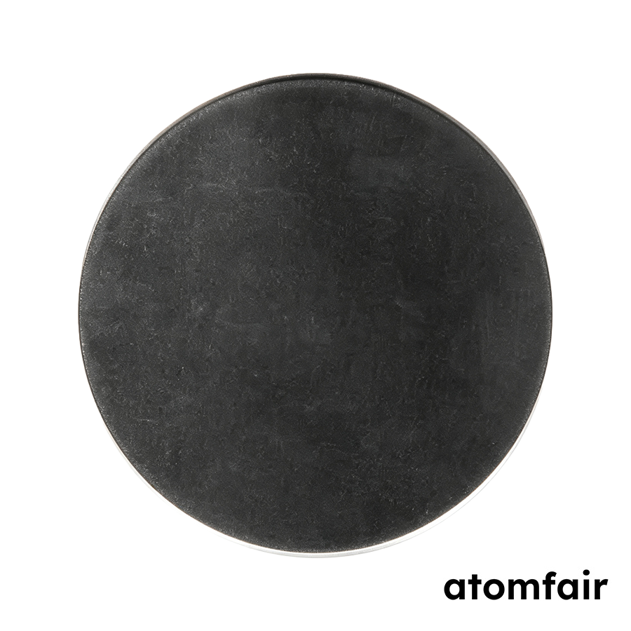
AlSiCu Sputtering Target 99.95% 2 in × 0.25 in ATOMFAIR®
$335.00 -
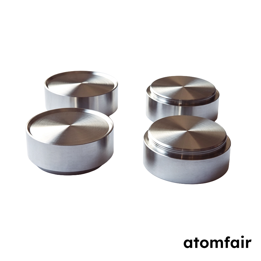
AlSm Aluminum Alloy Sputtering Target 99.9% 6 in ATOMFAIR®
$1,370.00 -
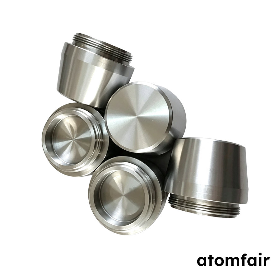
AlSn Alloy Sputtering Target 99.99% 5 in × 15 mm ATOMFAIR®
$1,325.00 -
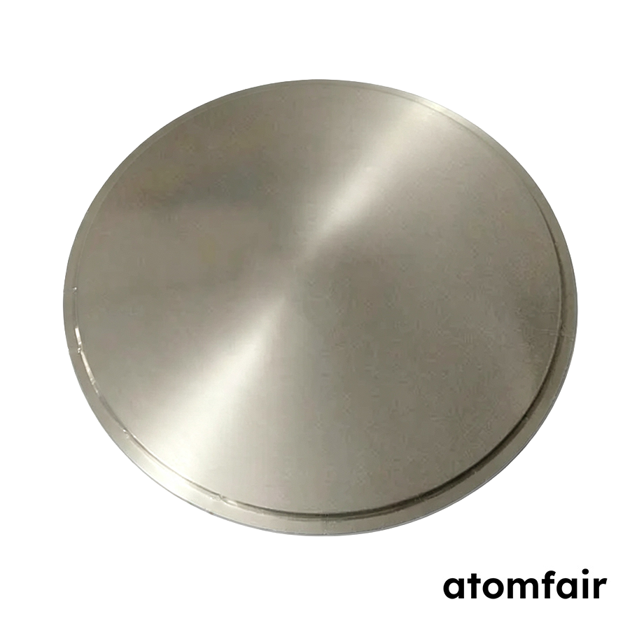
AlSnCu Sputtering Target 99.9% 3 in × 0.25 in ATOMFAIR®
$560.00 -
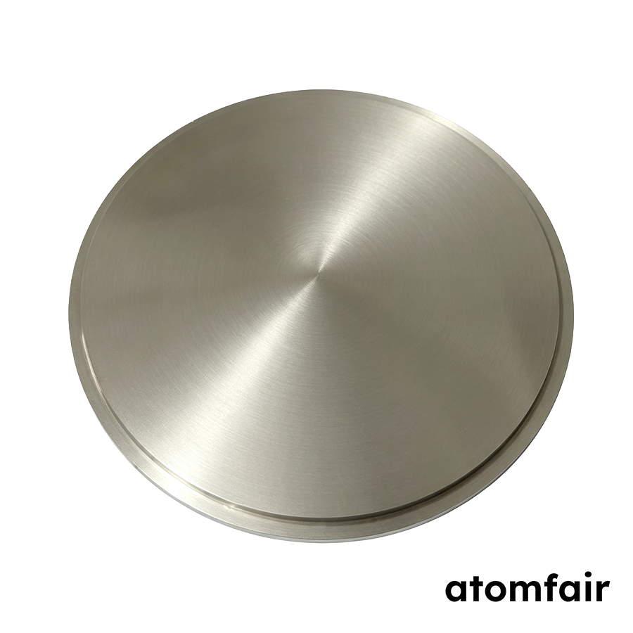
AlTi Sputtering Target 99.99% 5 in x 15 mm ATOMFAIR®
$1,325.00 -
Aluminium Al Evaporation Wire 99.99% 1.0 mm ATOMFAIR®
Price range: $310.00 through $1,000.00 -
Aluminium Al Evaporation Wire 99.99% 2.0 mm ATOMFAIR®
Price range: $310.00 through $1,000.00 -
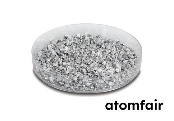
Aluminium Antimonide Powder 99.995% 500nm ATOMFAIR®
Price range: $700.00 through $6,000.00 -
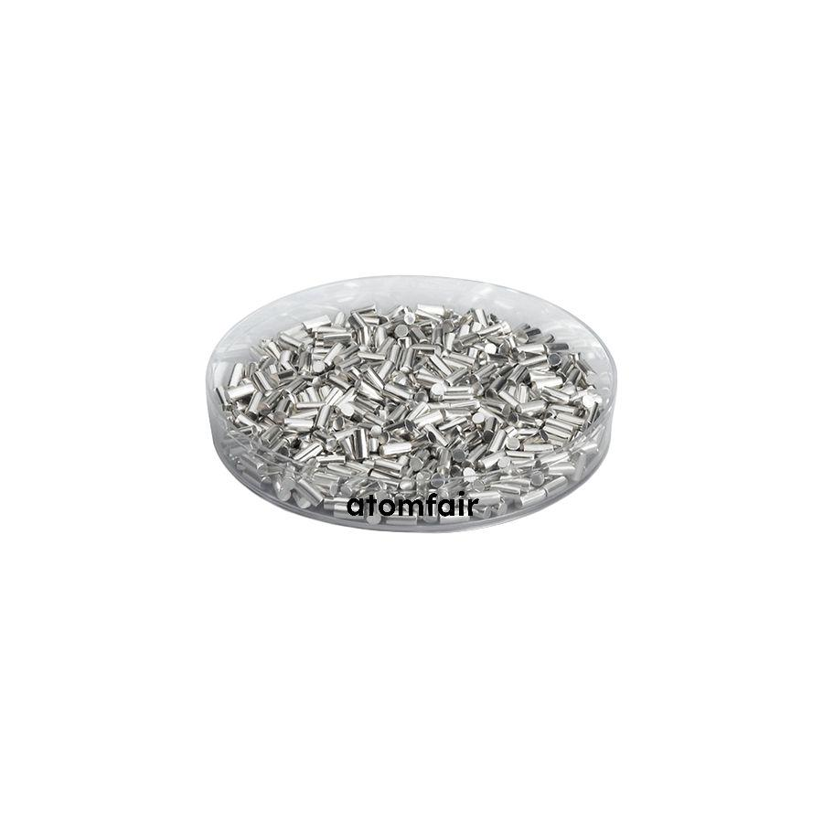
Aluminium Evaporation Pellets 99.99% 1-3 mm ATOMFAIR®
Price range: $310.00 through $1,000.00 -
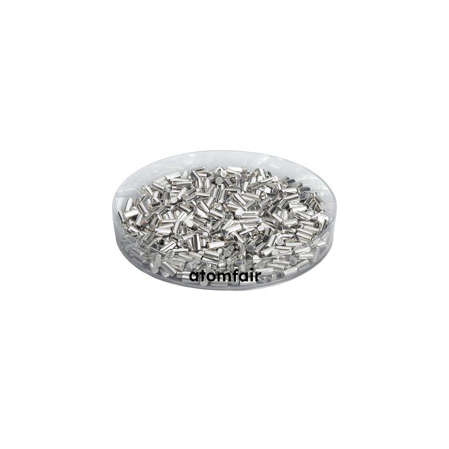
Aluminium Evaporation Pellets 99.99% 3-6 mm ATOMFAIR®
Price range: $310.00 through $1,000.00 -
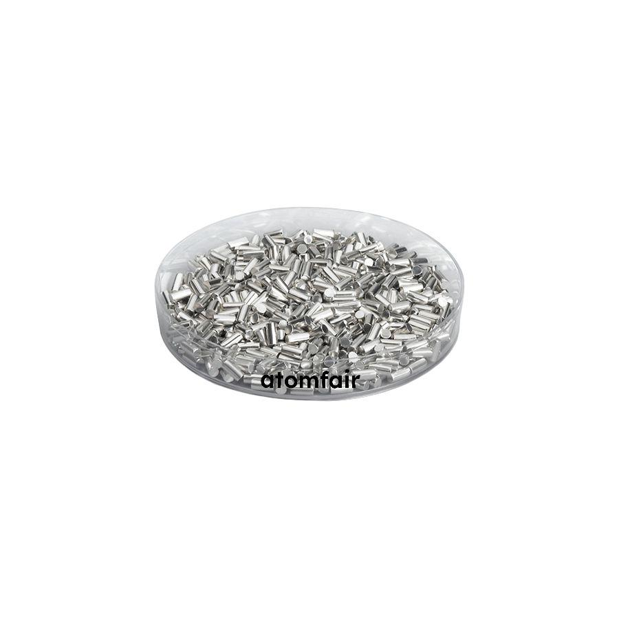
Aluminium Evaporation Pellets 99.999% 1-3 mm ATOMFAIR®
Price range: $200.00 through $1,400.00 -
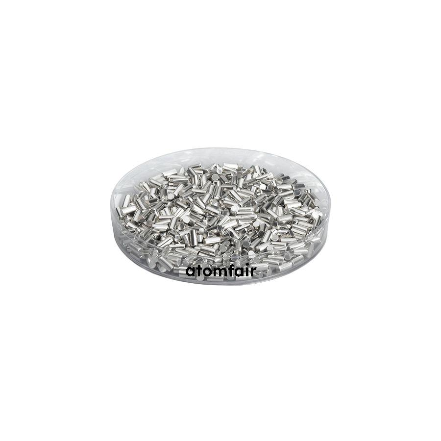
Aluminium Evaporation Pellets 99.999% 3-6 mm ATOMFAIR®
Price range: $200.00 through $1,400.00 -
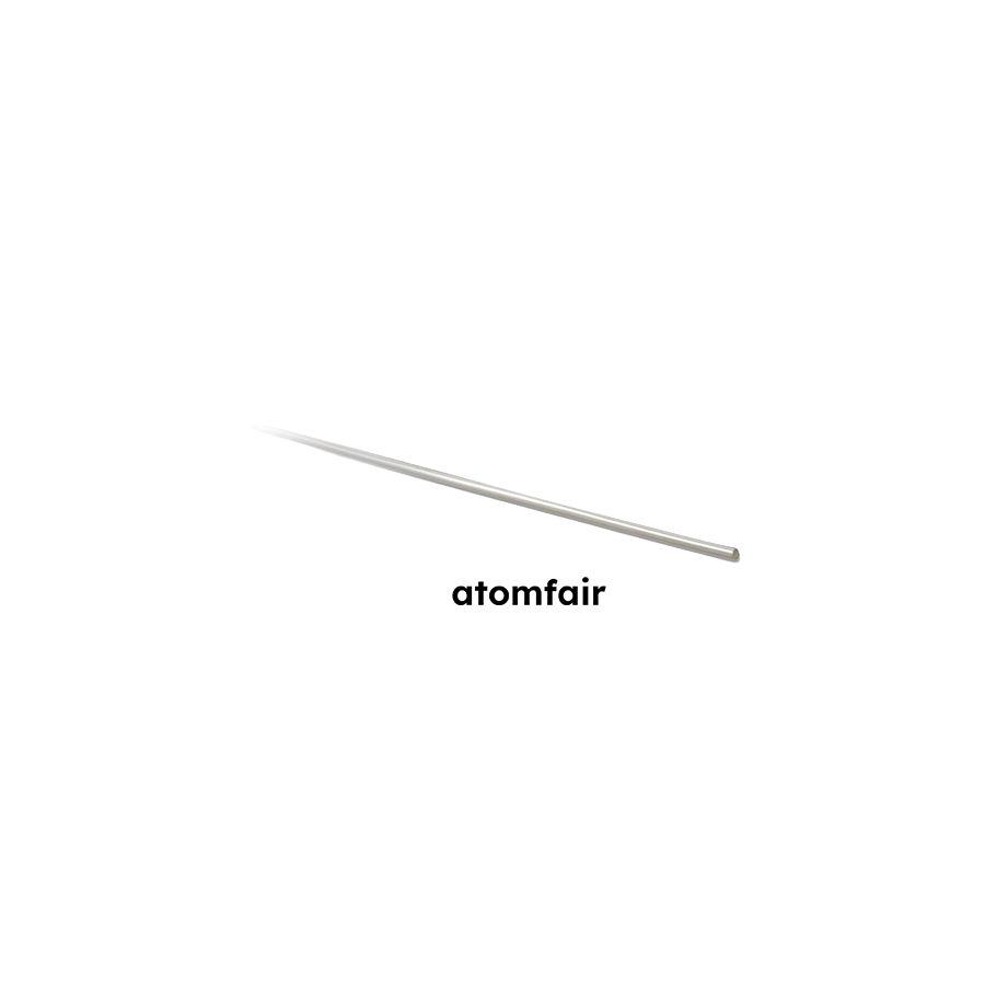
Aluminium Evaporation Wire 99.999% 1.0 mm ATOMFAIR®
Price range: $200.00 through $1,400.00 -
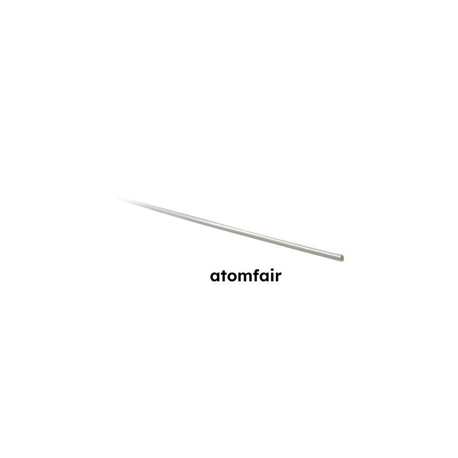
Aluminium Evaporation Wire 99.999%, Dia. 2.0 mm ATOMFAIR®
Price range: $200.00 through $1,400.00 -
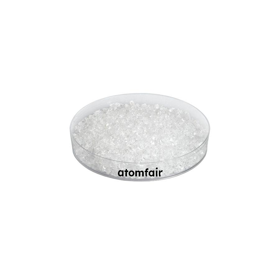
Aluminium Fluoride AlF3 Evaporation Pieces 99.99% ATOMFAIR®
Price range: $230.00 through $1,200.00 -
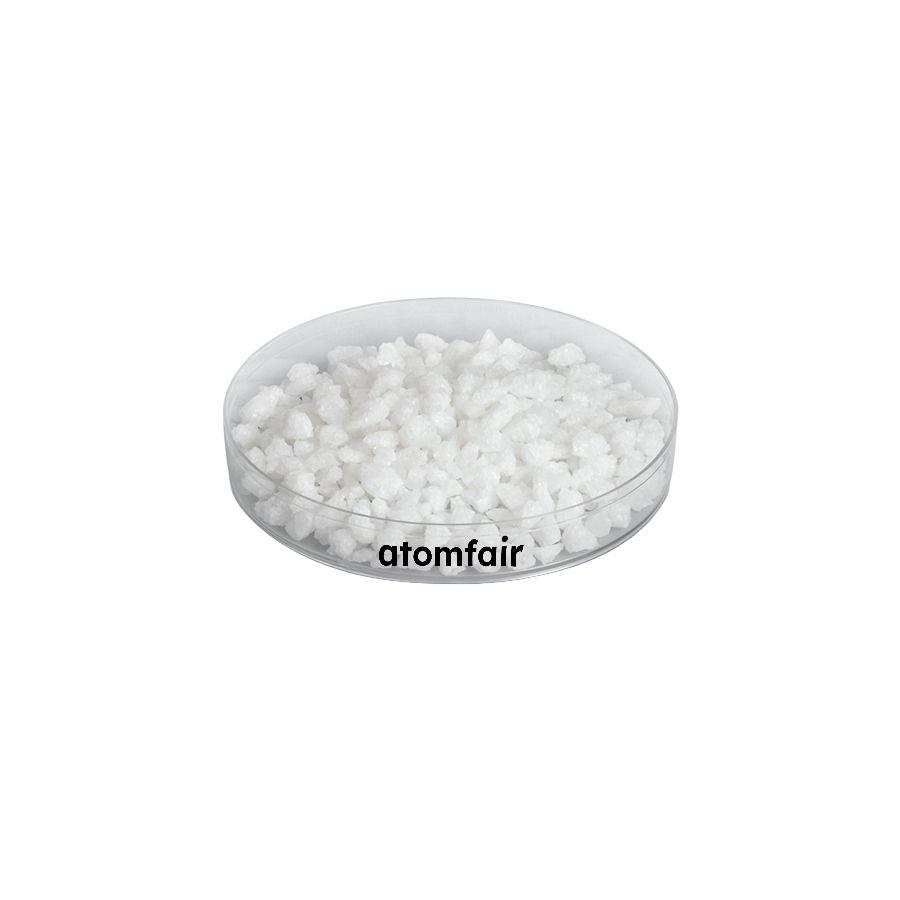
Aluminium Nitride (AlN) Powder 99.9% 10-25μm ATOMFAIR®
Price range: $370.00 through $2,700.00