|
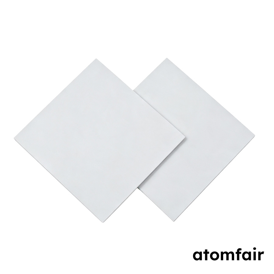
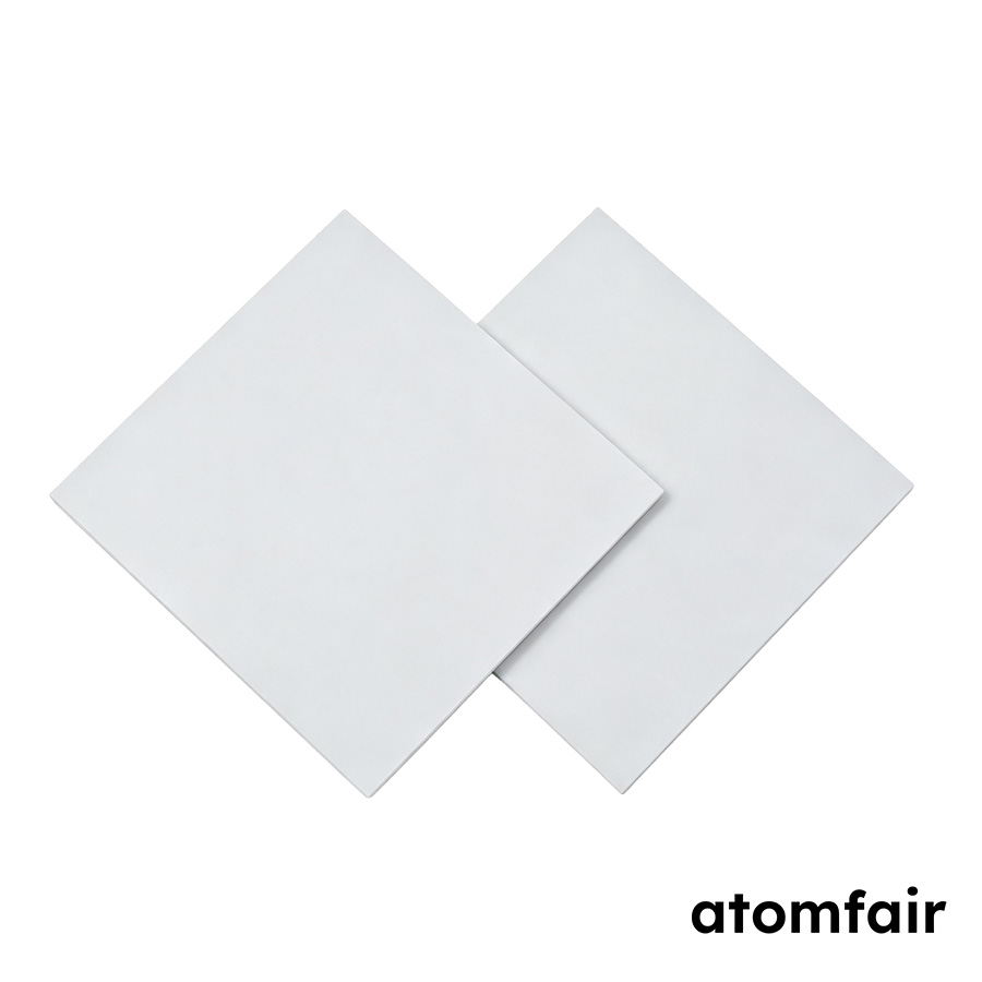
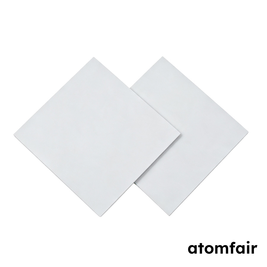
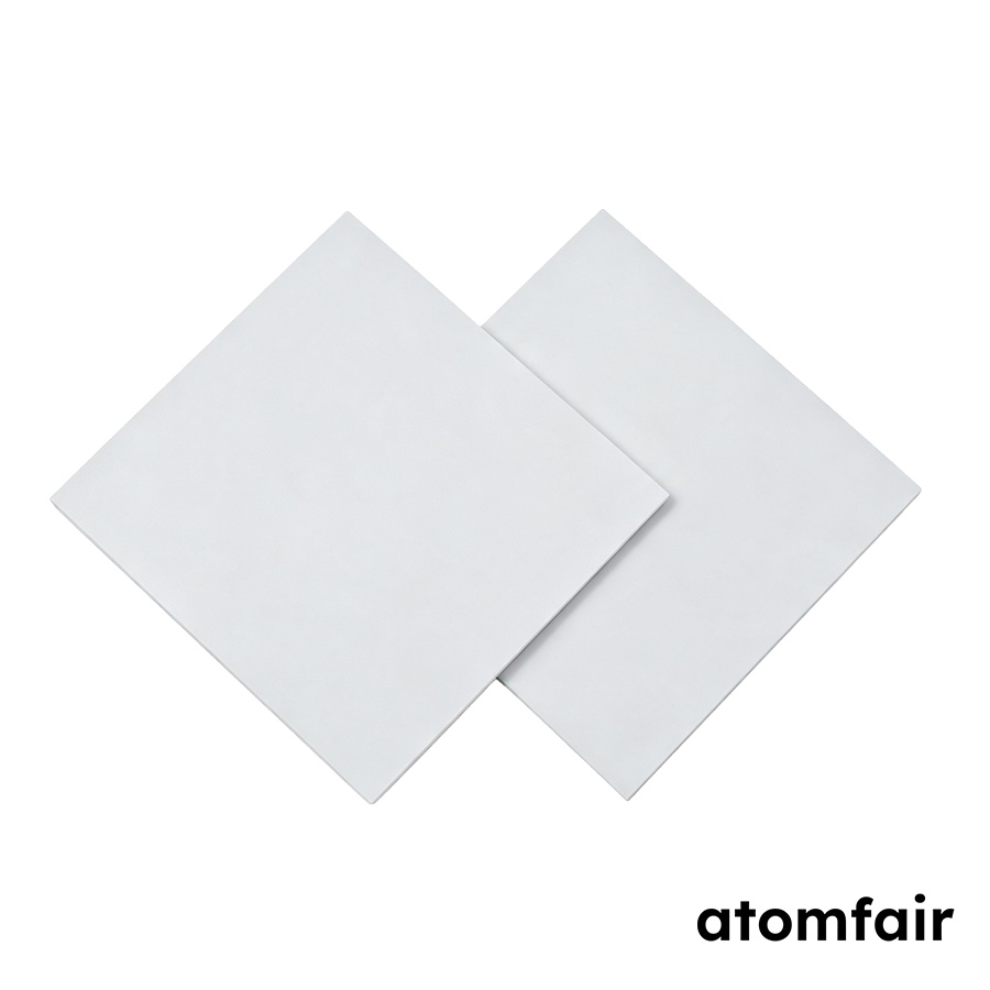
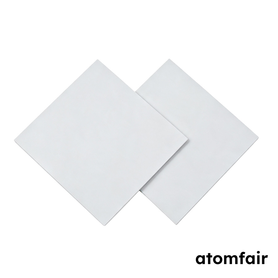
LSAT Single Crystal Substrate, (110), DSP (10 pcs/box)
Product Type: LSAT single crystal substrate
Research-grade laboratory product
|
|||||||||||||||||||||||||||||||||||||||||||||||||||
|
|||||||||||||||||||||||||||||||||||||||||||||||||||
|
LABORATORY PROCUREMENT SUPPORT
For material matching, specification review, model selection or configuration confirmation, contact our technical sales team.
E-MAIL: inquiry@atomfair.com
|
|||||||||||||||||||||||||||||||||||||||||||||||||||
|
Manufacturer: Atomfair LLC
Brand: ATOMFAIR®
|
The substrate material must be matched to the target thin-film or device workflow to prevent lattice or thermal expansion mismatch. Orientation and surface finish are critical for epitaxial quality; the substrate must be stored in a clean, particle-free environment to preserve surface integrity.
- Lattice Matching: Confirm that the LSAT lattice constant and thermal expansion coefficient are compatible with the intended thin-film material.
- Orientation Tolerance: Verify that the substrate orientation is within ±0.5° of the specified (110) plane to ensure proper epitaxial alignment.
- Surface Roughness: Ensure the surface roughness (Ra) is below 5 Å to minimize defect nucleation during film growth.
- Defect Inspection: Inspect the substrate for twin-free and domain-free condition as specified for high-quality epitaxy.
- Contamination Control: Handle the substrate with cleanroom gloves and store in a sealed container to avoid surface contamination.
What is the significance of the ±0.5° orientation tolerance for LSAT (110) substrates in epitaxial thin-film growth?
The ±0.5° orientation tolerance ensures precise crystallographic alignment for epitaxial deposition. The LSAT substrate has a cubic structure with lattice constant a = 3.868Å, and the tight orientation tolerance minimizes misorientation that could introduce defects in the overlaid thin film.
What high-temperature deposition processes are compatible with LSAT (110) substrates?
LSAT substrates are compatible with high-temperature processes such as PLD and MBE due to a melting point of 1840°C and a thermal expansion coefficient of 10 × 10⁻⁶/K, which reduces thermal stress during heating and cooling.
What handling precautions are required for LSAT (110) substrates with DSP surface finish to maintain a surface roughness below 5Å?
The DSP finish requires cleanroom handling to avoid contamination and scratches. The substrate's 0.5 mm thickness makes it fragile, so it should be handled with tweezers and stored in a clean, dry container to preserve the Ra < 5Å surface quality.
LSAT (110) single crystal substrate with DSP finish, available in 10×10×0.5 mm and 5×5×0.5 mm sizes, offers a cubic lattice constant of 3.868 Å, high melting point of 1840°C, and twin-free, low-roughness surface suitable for epitaxial thin-film growth of complex oxide materials.
Positive
- Twin-free and domain-free crystal: The substrate is twin-free with no visible domains, ensuring a structurally uniform surface for epitaxial thin-film deposition without defect propagation.
- Low surface roughness Ra < 5Å: Surface roughness below 5Å provides an atomically smooth substrate, minimizing interface scattering and promoting high-quality film growth.
Trade-offs
- Requires material matching verification: The substrate material (LSAT) and crystal family must be confirmed compatible with the target thin-film material and device workflow before purchase to avoid lattice mismatch or performance issues.
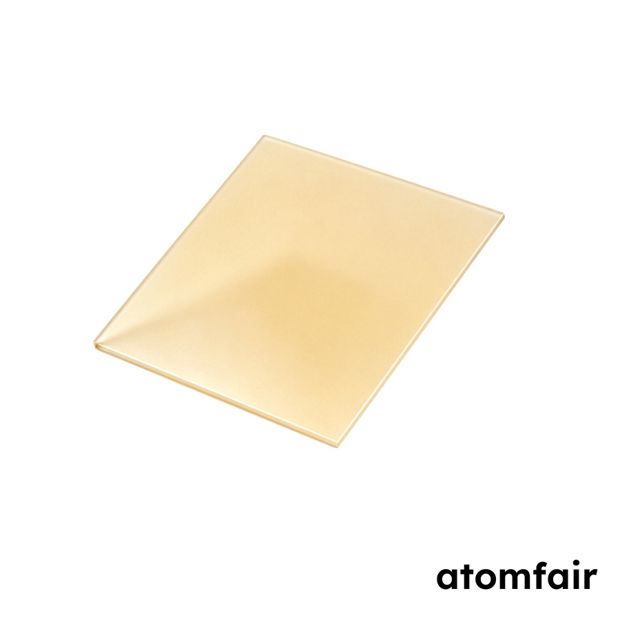
- Annealing-dependent optical appearance: The substrate color varies from dark brown to light yellow depending on annealing condition, which may affect optical transmission measurements or require specified annealing history for consistent results.
Every advanced material, component, equipment, and instrument in our catalog is backed by rigorous testing. We maintain strict internal quality management frameworks and align with CE conformity metrics to deliver transparent, reproducible performance data via our public open-science repository.
To request raw batch performance data, submit formal vendor registration paperwork, or execute a fast-turnaround R&D manufacturing loop, contact us at inquiry@atomfair.com.
Item is dispatched under the Atomfair Shipping & Delivery Framework (Free worldwide shipping on orders over $59 USD excl. heavy equipment). Return is governed by the Atomfair Return & Refund Policy (7-day technical return window).