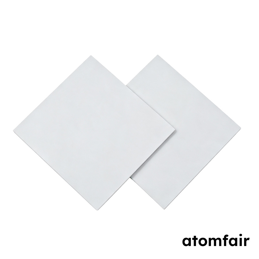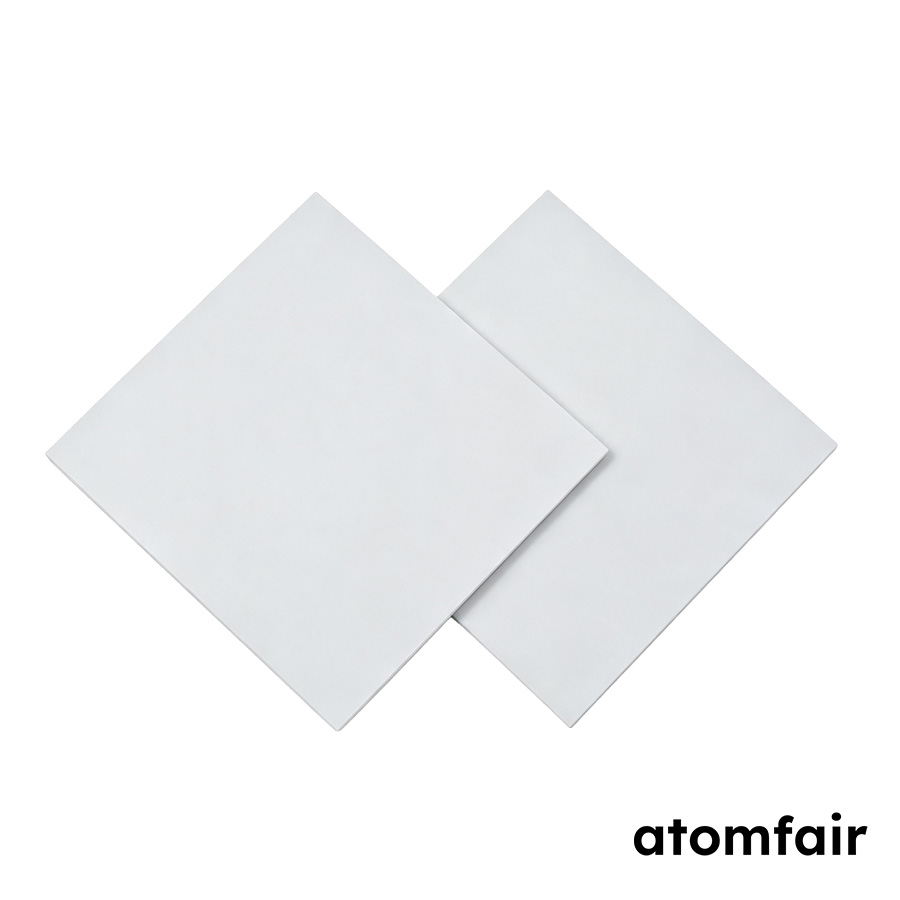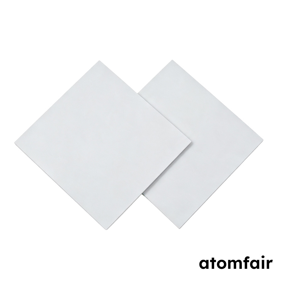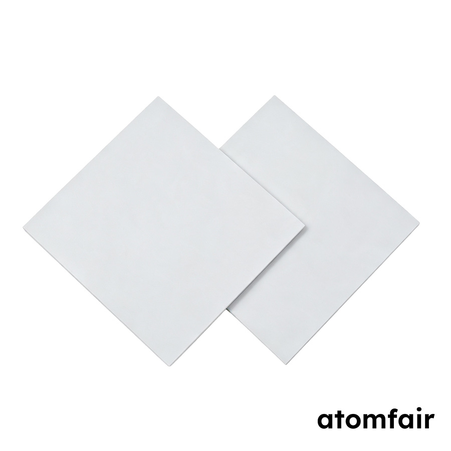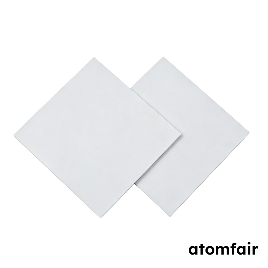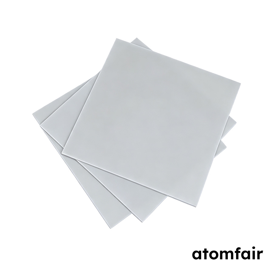
Aluminum Nitride Ceramic Substrate, 20 mm x 20 mm x 1 mm, Pack of 10Product Type: Technical ceramic substrate
Research-grade laboratory product
|
|||||||||||||||||||||||||||||||||
|
|||||||||||||||||||||||||||||||||
|
LABORATORY PROCUREMENT SUPPORT
For model selection, accessory matching, platform compatibility or configuration confirmation, contact our technical sales team.
E-MAIL: inquiry@atomfair.com
|
|||||||||||||||||||||||||||||||||
|
Supplier: Atomfair
Brand: ATOMFAIR®
|
This substrate exhibits high thermal conductivity above 170 W/(m·K) and a thermal expansion coefficient close to silicon, requiring careful thermal management during power module integration. The material's surface roughness of 0.2–0.3 μm and flexural strength above 400 MPa impose specific handling and processing conditions to avoid mechanical failure.
- Thermal Management Requirement: The substrate's high thermal conductivity necessitates controlled heat dissipation pathways to prevent thermal stress during soldering or sintering processes.
- Mechanical Handling Constraint: The specified surface roughness and flexural strength require careful handling to avoid chipping or cracking during cutting or metallization steps.
- Dielectric Integrity Constraint: The breakdown voltage of ≥15 kV/mm mandates that the substrate surface remain free of conductive contaminants to maintain insulation performance.
This procedure outlines the cleaning and surface preparation steps required before applying metallization layers to the aluminum nitride substrate. Proper preparation ensures adhesion and prevents delamination during subsequent thermal processing.
Required Equipment: Ultrasonic cleaner, Isopropyl alcohol (IPA), Deionized water, Nitrogen blow gun
- Clean substrate surface
Immerse the substrate in isopropyl alcohol and sonicate for 10 minutes to remove organic residues. - Rinse with deionized water
Rinse the substrate thoroughly with deionized water to remove any residual IPA and dissolved contaminants. - Dry the substrate
Blow dry the substrate with filtered nitrogen gas to prevent water spots and ensure a clean surface. - Verify surface cleanliness
Inspect the substrate under a microscope to confirm no visible particles or stains remain before proceeding to metallization.
How does the thermal conductivity of this aluminum nitride substrate compare to alumina, and what specific value is guaranteed?
This aluminum nitride ceramic substrate provides thermal conductivity above 170 W/(m·K) at 25 °C, which is approximately 7–10 times higher than alumina ceramic. This high thermal conductivity, combined with a thermal expansion coefficient close to silicon, makes it suitable for power module and electronic component heat-dissipation applications.
What are the mechanical and electrical constraints for integrating this 20 mm x 20 mm x 1 mm substrate into a power module design?
The substrate has a flexural strength greater than 400 MPa, a Vickers hardness of 11 GPa, and a Young modulus of 320 GPa, providing robust mechanical support. Electrically, it offers a DC breakdown voltage of at least 15 kV/mm and a surface roughness Ra of 0.2–0.3 µm, which supports reliable insulation and low dielectric loss for high-voltage or high-frequency insulating substrate use.
What handling or procurement steps are required to confirm the exact specifications for this aluminum nitride substrate before ordering?
Before ordering, buyers must verify size tolerance, thickness requirement, material grade, surface finish, and package format for this specific 20 mm x 20 mm x 1 mm, pack-of-10 configuration. Additionally, any polishing, coating, metallization, or custom-shape needs should be confirmed with the technical sales team to ensure compatibility with the intended application.
This 20 mm x 20 mm x 1 mm aluminum nitride ceramic substrate provides a measured thermal conductivity greater than 170 W/(m·K), approximately 7-10 times higher than alumina, with a thermal expansion coefficient matching silicon for direct substrate mounting in power modules. The substrate requires careful handling due to its high Vickers hardness of 11 GPa and flexural strength exceeding 400 MPa, which complicates post-processing such as cutting or drilling without diamond tooling.
Positive
- High thermal conductivity vs alumina: Thermal conductivity above 170 W/(m·K) is 7-10 times higher than alumina ceramic, enabling efficient heat spreading and dissipation in power electronic and LED substrate applications.
- CTE matched to silicon: Thermal expansion coefficient close to silicon reduces thermomechanical stress during soldering or brazing in power module assembly, improving long-term reliability.
Trade-offs
- Hardness limits post-processing: Vickers hardness of 11 GPa and flexural strength >400 MPa require diamond tooling or laser cutting for shaping or drilling, demanding specialized laboratory equipment.
- Surface finish verification needed: Surface roughness Ra of 0.2-0.3 μm is specified but may require confirmation for thin-film metallization or direct bond copper processes, which have tighter flatness requirements.
Every advanced material, component, equipment, and instrument in our catalog is backed by rigorous testing. We maintain strict internal quality management frameworks and align with CE conformity metrics to deliver transparent, reproducible performance data via our public open-science repository.
To request raw batch performance data, submit formal vendor registration paperwork, or execute a fast-turnaround R&D manufacturing loop, contact us at inquiry@atomfair.com.
Item is dispatched under the Atomfair Shipping & Delivery Framework (Free worldwide shipping on orders over $59 USD excl. heavy equipment). Return is governed by the Atomfair Return & Refund Policy (7-day technical return window).