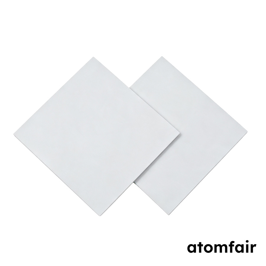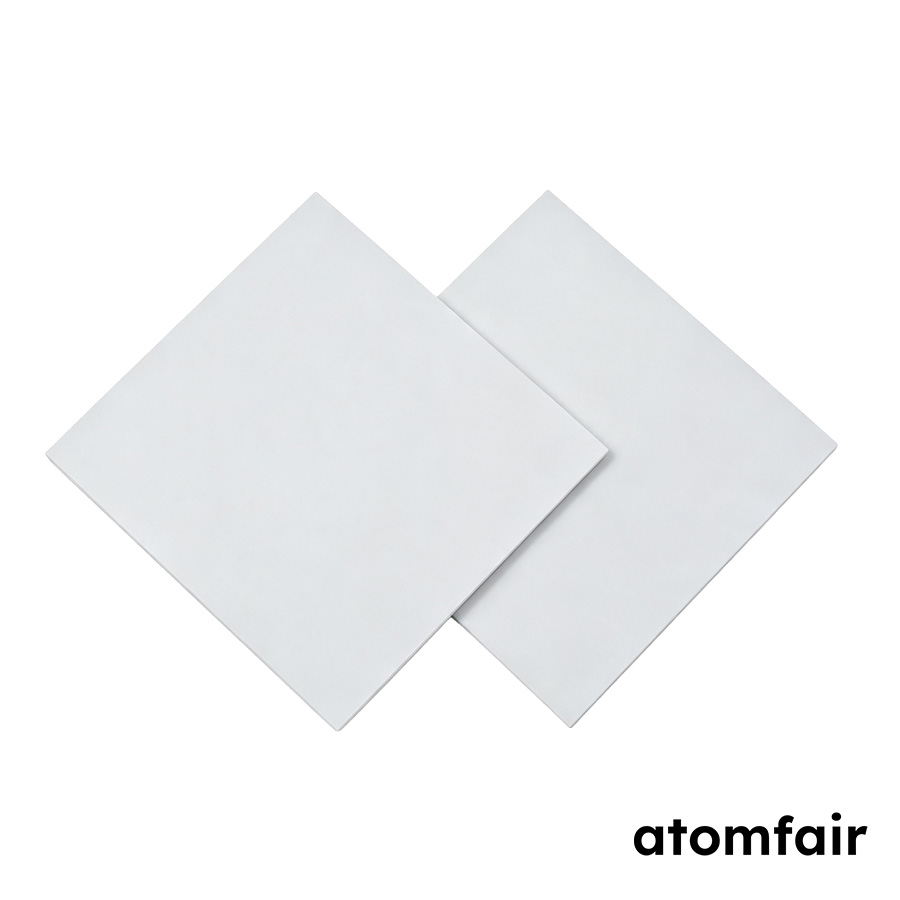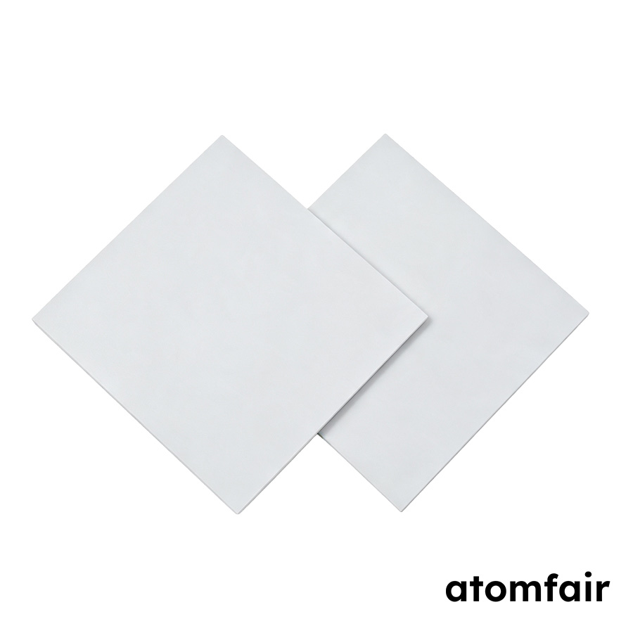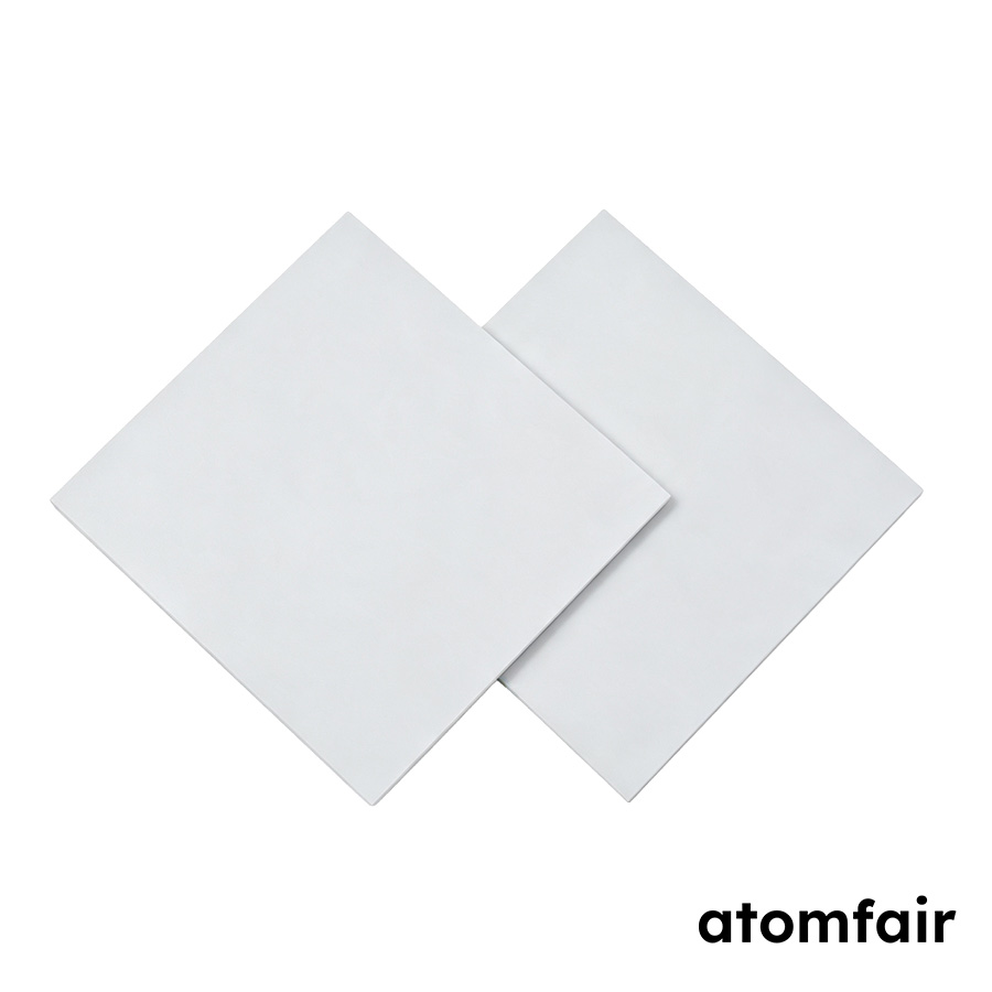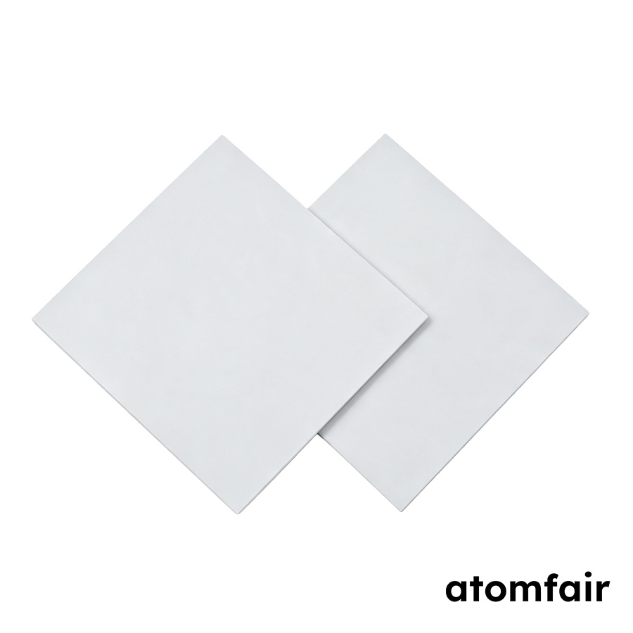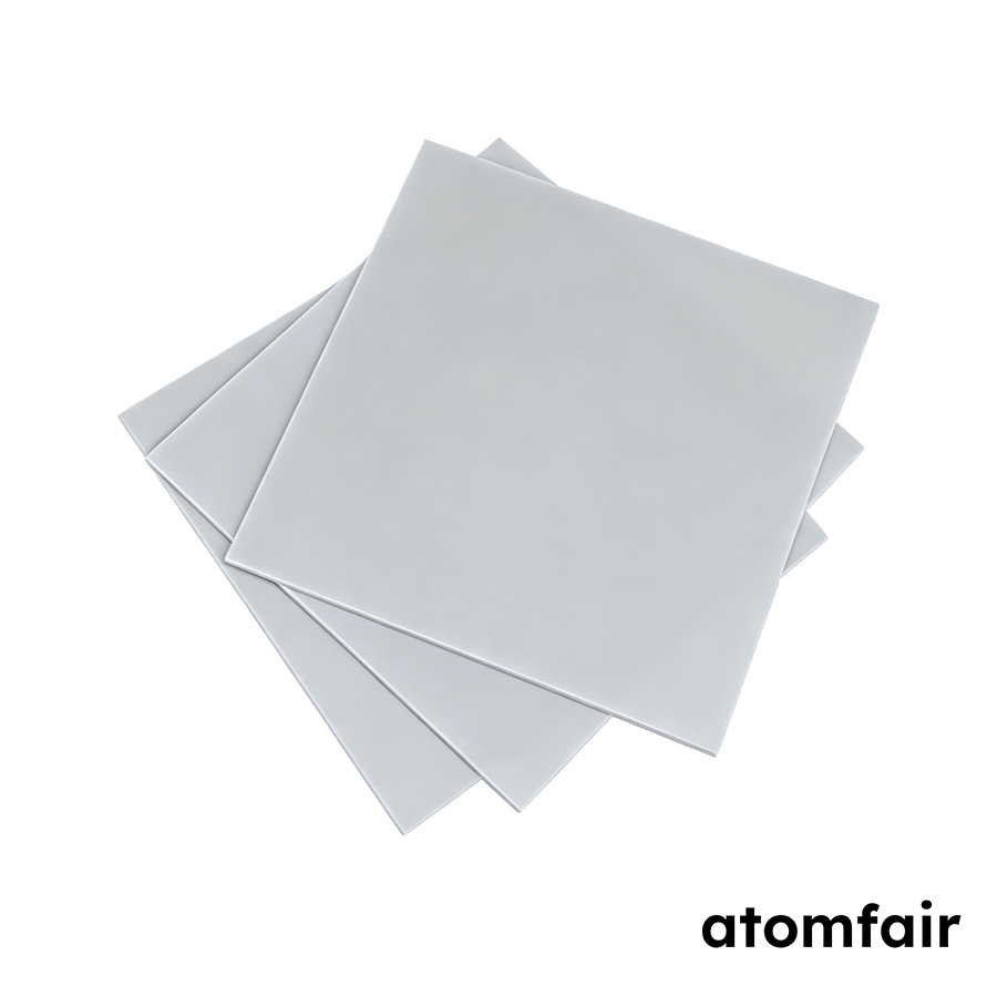
Aluminum Nitride Ceramic Substrate, 10 mm x 10 mm x 0.63 mm, Pack of 10Product Type: Technical ceramic substrate
Research-grade laboratory product
|
|||||||||||||||||||||||||||||||||
|
|||||||||||||||||||||||||||||||||
|
LABORATORY PROCUREMENT SUPPORT
For model selection, accessory matching, platform compatibility or configuration confirmation, contact our technical sales team.
E-MAIL: inquiry@atomfair.com
|
|||||||||||||||||||||||||||||||||
|
Supplier: Atomfair
Brand: ATOMFAIR®
|
This substrate requires careful handling to prevent surface contamination or mechanical damage that could compromise thermal and electrical performance. The material's high hardness and brittleness necessitate controlled processing environments to avoid chipping or fracture during cutting, drilling, or metallization.
- Surface Integrity: Maintain the as-received surface roughness of 0.2–0.3 µm by avoiding abrasive contact or chemical exposure that could alter the finish.
- Thermal Management: Ensure adequate heat sinking during soldering or brazing to prevent thermal shock, as the substrate's high thermal conductivity can induce rapid temperature gradients.
- Dielectric Safety: Do not exceed the DC breakdown voltage of 15 kV/mm to avoid catastrophic dielectric failure through the ceramic body.
This procedure outlines safe handling and preparation steps for the aluminum nitride ceramic substrate prior to device assembly. Follow these steps to maintain substrate integrity and avoid contamination or mechanical damage.
Required Equipment: Cleanroom-grade gloves, Isopropyl alcohol and lint-free wipes, Diamond scribe or laser cutter
- Inspect substrate
Visually examine each substrate under bright light for cracks, chips, or surface defects before any processing. - Clean surface
Wipe the substrate with isopropyl alcohol and a lint-free wipe to remove particulate contamination without scratching the surface. - Dice or cut substrate
Use a diamond scribe or laser cutter to score and break the substrate along desired dimensions, applying minimal force to prevent fracture. - Store prepared substrates
Place cut substrates in a clean, dry container with foam or gel-pak separation to avoid edge chipping during storage.
How does the thermal conductivity of this Atomfair aluminum nitride substrate compare to alumina for high-power electronic heat dissipation?
This AlN substrate provides thermal conductivity above 170 W/(m·K), which is approximately 7–10 times higher than typical alumina ceramic. This makes it significantly more effective for heat dissipation in power modules and electronic components.
Is the thermal expansion coefficient of this 10 mm x 10 mm x 0.63 mm AlN substrate compatible with direct bonding to silicon devices?
Yes, the thermal expansion of this aluminum nitride ceramic is close to that of silicon, making it suitable for power module and electronic component workflows. This compatibility reduces thermal stress during soldering or direct bonding.
What surface roughness is specified for this AlN substrate, and does it support thin-film metallization or direct bond copper (DBC) processes?
The surface roughness Ra is specified at 0.2–0.3 μm, which is suitable for thin-film metallization and DBC processes. This smooth finish promotes good adhesion for subsequent coating or metallization layers.
This 10 mm x 10 mm x 0.63 mm aluminum nitride ceramic substrate delivers thermal conductivity above 170 W/(m·K), approximately 7–10× that of alumina, with a thermal expansion coefficient matched to silicon, making it suitable for high-power electronic substrate applications requiring efficient heat dissipation.
Positive
- High thermal conductivity: Thermal conductivity exceeds 170 W/(m·K) at 25 °C, approximately 7–10 times higher than alumina, enabling efficient heat spreading in power modules and electronic assemblies.
- Matched CTE to silicon: Thermal expansion coefficient is close to silicon, reducing thermomechanical stress during thermal cycling in semiconductor and power-device attachment processes.
Trade-offs
- Surface roughness Ra 0.2–0.3 µm: As-fired surface roughness of 0.2–0.3 µm may require additional polishing or metallization steps for thin-film or fine-line circuit deposition, adding process complexity.
- Configuration confirmation required: Size tolerance, thickness, material grade, and surface finish must be verified with the supplier before ordering, as the product is supplied as an independent substrate without pre-applied coatings or metallization layers.
Every advanced material, component, equipment, and instrument in our catalog is backed by rigorous testing. We maintain strict internal quality management frameworks and align with CE conformity metrics to deliver transparent, reproducible performance data via our public open-science repository.
To request raw batch performance data, submit formal vendor registration paperwork, or execute a fast-turnaround R&D manufacturing loop, contact us at inquiry@atomfair.com.
Item is dispatched under the Atomfair Shipping & Delivery Framework (Free worldwide shipping on orders over $59 USD excl. heavy equipment). Return is governed by the Atomfair Return & Refund Policy (7-day technical return window).