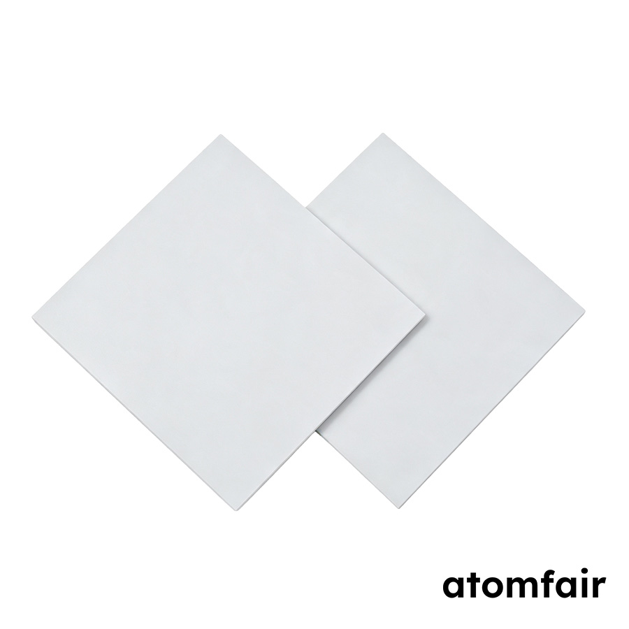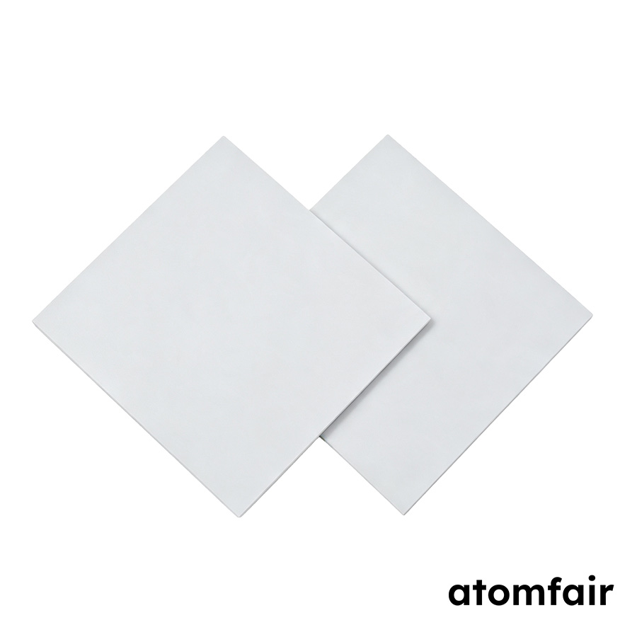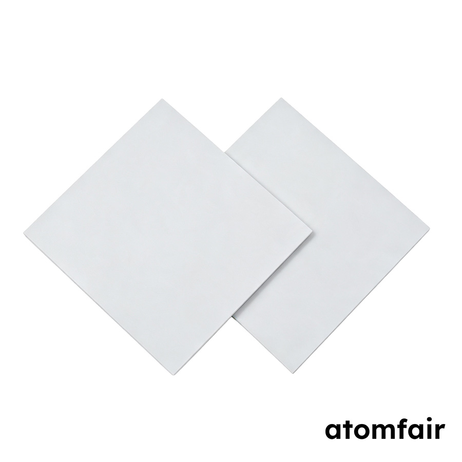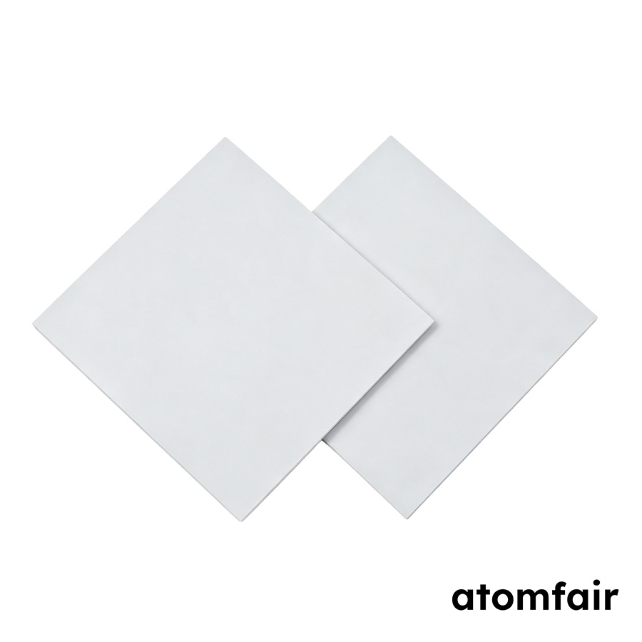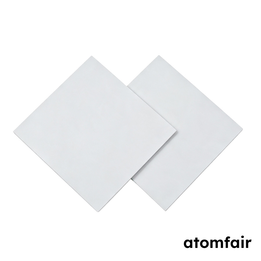
96% Alumina Ceramic Substrate, 150 mm x 150 mm x 0.635 mm, Pack of 10Product Type: Technical ceramic substrate
Research-grade laboratory product
|
|||||||||||||||||||||||||||||||||
|
|||||||||||||||||||||||||||||||||
|
LABORATORY PROCUREMENT SUPPORT
For model selection, accessory matching, platform compatibility or configuration confirmation, contact our technical sales team.
E-MAIL: inquiry@atomfair.com
|
|||||||||||||||||||||||||||||||||
|
Supplier: Atomfair
Brand: ATOMFAIR®
|
What is the surface roughness and flexural strength of the 96% alumina ceramic substrate 150 mm x 150 mm x 0.635 mm?
The substrate has a surface roughness of Ra 0.15–0.30 µm and a flexural strength greater than 350 MPa. These specifications, combined with a Vickers hardness of 14 GPa and a density of ≥3.70 g/cm³, indicate suitability for applications requiring high mechanical integrity and a smooth surface for thin-film deposition or metallization.
Can this 96% alumina substrate be used for high-voltage isolation in power electronics?
Yes, the substrate provides a breakdown voltage of ≥15 kV/mm, making it suitable for high-voltage isolation in power modules and thick-film hybrid circuits. Its low dielectric constant and low dielectric loss, combined with a thermal conductivity >24 W/(m·K), support efficient heat dissipation while maintaining electrical insulation.
What handling or storage precautions are recommended for the 96% alumina ceramic substrate?
The substrate is a dense, white ceramic with high hardness (14 GPa) but is brittle; handle with care to avoid chipping or cracking. Store in a clean, dry environment to prevent surface contamination, as the Ra 0.15–0.30 µm finish is critical for subsequent processing steps such as metallization or thin-film deposition.
This 96% alumina ceramic substrate (150 mm x 150 mm x 0.635 mm, pack of 10) delivers high mechanical strength (>350 MPa flexural), electrical insulation (≥15 kV/mm breakdown), low dielectric loss, and thermal conductivity >24 W/(m·K), making it suitable for high-temperature, corrosive, or electrically demanding lab applications. The 0.15-0.30 μm surface roughness and dense white microstructure support consistent thin-film deposition or bonding, though machining post-purchase requires specialized diamond tooling.
Positive
- High mechanical and dielectric strength: Flexural strength >350 MPa and breakdown voltage ≥15 kV/mm ensure structural integrity under mechanical load and high-voltage isolation, critical for power electronics or vacuum chamber feedthroughs.
- Thermal and chemical resilience: Thermal conductivity >24 W/(m·K) combined with good corrosion resistance and chemical stability allows use in high-temperature or aggressive solvent environments without degradation.
Trade-offs
- Brittle under point loading: As a ceramic, the substrate is brittle; although flexural strength exceeds 350 MPa, localized impact or uneven clamping can cause fracture without ductile deformation, requiring careful handling.
- Machining requires diamond tooling: The 14 GPa Vickers hardness makes post-fabrication cutting, drilling, or shaping impractical without diamond-coated tools and coolant, limiting on-site customization.
Every advanced material, component, equipment, and instrument in our catalog is backed by rigorous testing. We maintain strict internal quality management frameworks and align with CE conformity metrics to deliver transparent, reproducible performance data via our public open-science repository.
To request raw batch performance data, submit formal vendor registration paperwork, or execute a fast-turnaround R&D manufacturing loop, contact us at inquiry@atomfair.com.
Item is dispatched under the Atomfair Shipping & Delivery Framework (Free worldwide shipping on orders over $59 USD excl. heavy equipment). Return is governed by the Atomfair Return & Refund Policy (7-day technical return window).