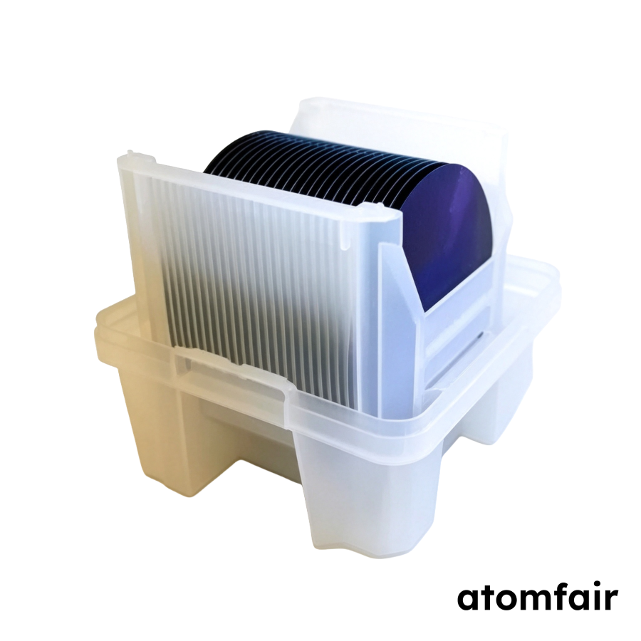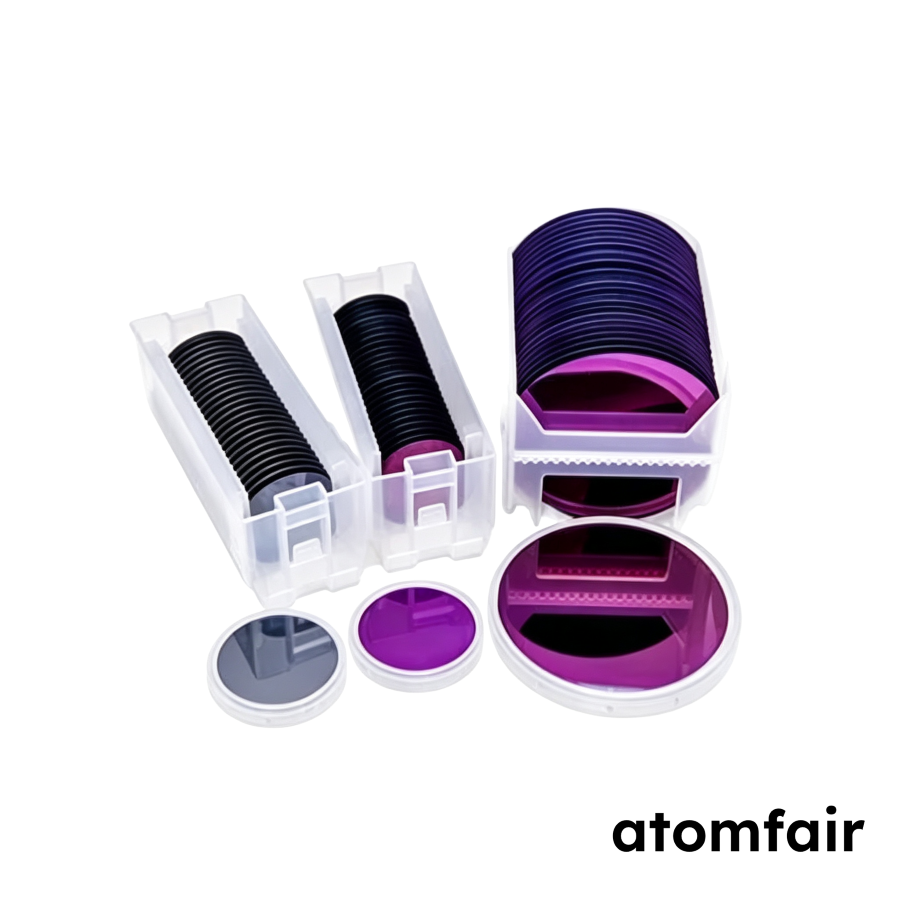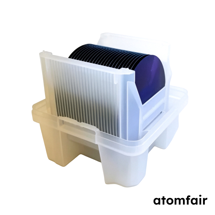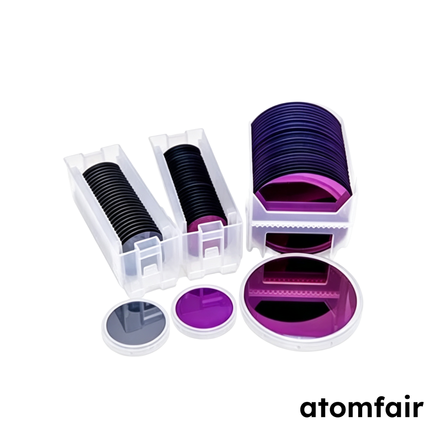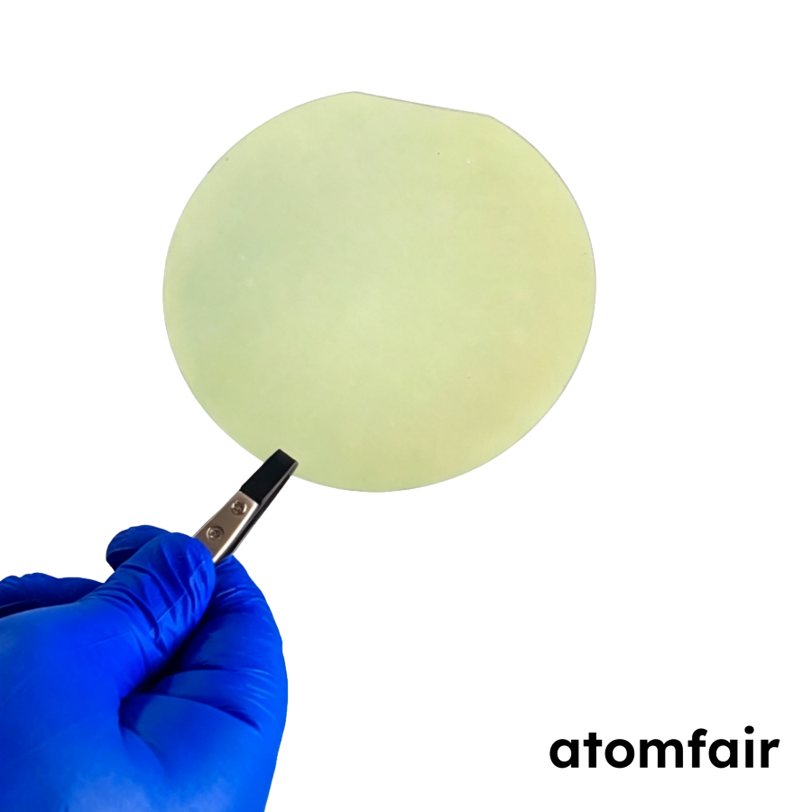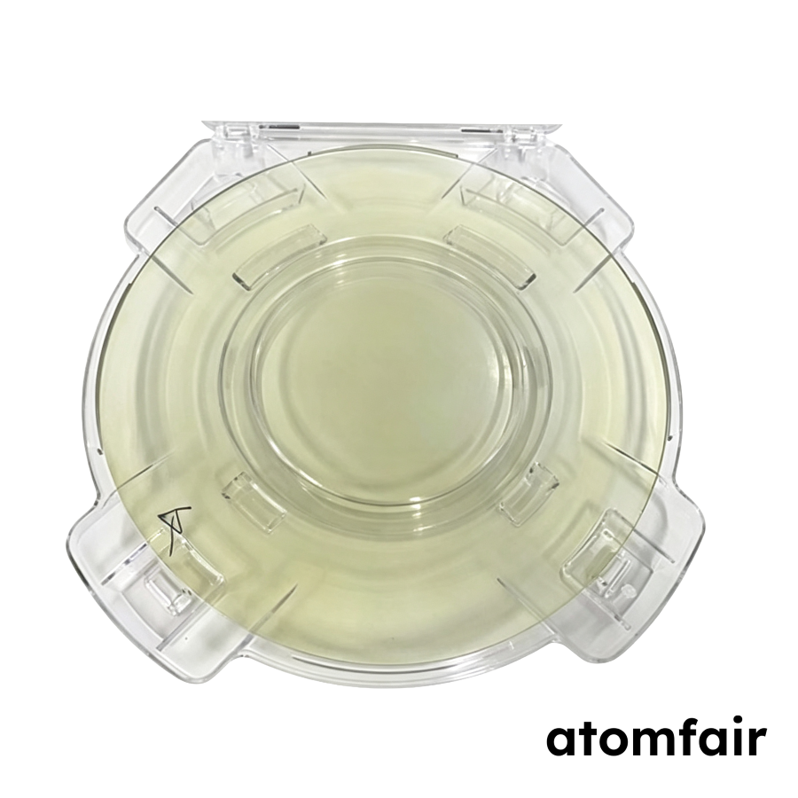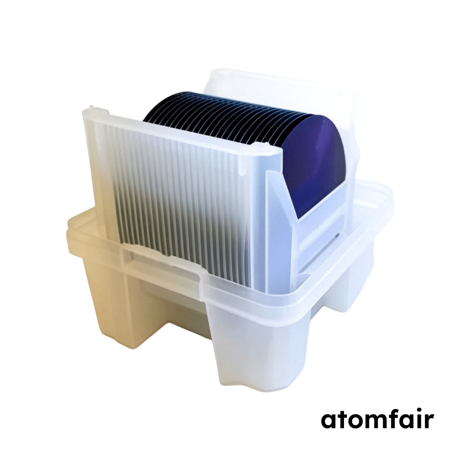
12 Inch Single-Side Oxidation Silicon Nitride WaferProduct Type: Silicon nitride wafer
Research-grade laboratory product
|
|||||||||||||||||||||||||||
|
|||||||||||||||||||||||||||
|
LABORATORY PROCUREMENT SUPPORT
For model selection, substrate matching or configuration confirmation, contact our technical sales team.
E-MAIL: inquiry@atomfair.com
|
|||||||||||||||||||||||||||
|
Supplier: Atomfair
Brand: ATOMFAIR®
|
What is the maximum SiO2 film thickness available for the 12-inch single-side oxidation silicon nitride wafer?
The SiO2 film thickness ranges from 5 nm to 10 μm, with a conventional thickness of 100-500 nm. Both oxidation furnace and PECVD processing routes are available for specification confirmation.
Which crystal orientations and conductivity types are supported for this 12-inch silicon nitride wafer?
Crystal orientations <100>, <111>, and <110> are listed. Conductivity types include N-type, P-type, or undoped high-resistivity, with resistivity bands from heavily doped (< 0.001 ohm.cm) to undoped (> 100-20000 ohm.cm).
What processing methods are available for the SiO2 film on this wafer?
Both oxidation furnace and PECVD processing routes are listed for the SiO2 film. The requested processing route must be stated during quotation confirmation to ensure compatibility with the intended application.
Every advanced material, component, equipment, and instrument in our catalog is backed by rigorous testing. We maintain strict internal quality management frameworks and align with CE conformity metrics to deliver transparent, reproducible performance data via our public open-science repository.
To request raw batch performance data, submit formal vendor registration paperwork, or execute a fast-turnaround R&D manufacturing loop, contact us at inquiry@atomfair.com.
Item is dispatched under the Atomfair Shipping & Delivery Framework (Free worldwide shipping on orders over $59 USD excl. heavy equipment). Return is governed by the Atomfair Return & Refund Policy (7-day technical return window).