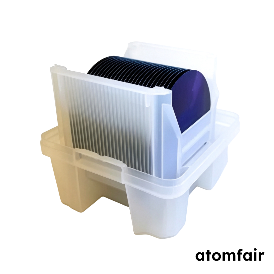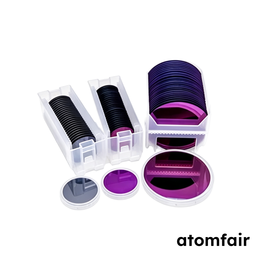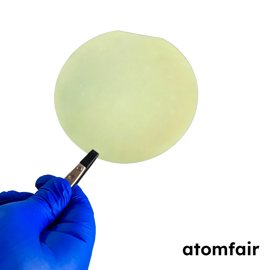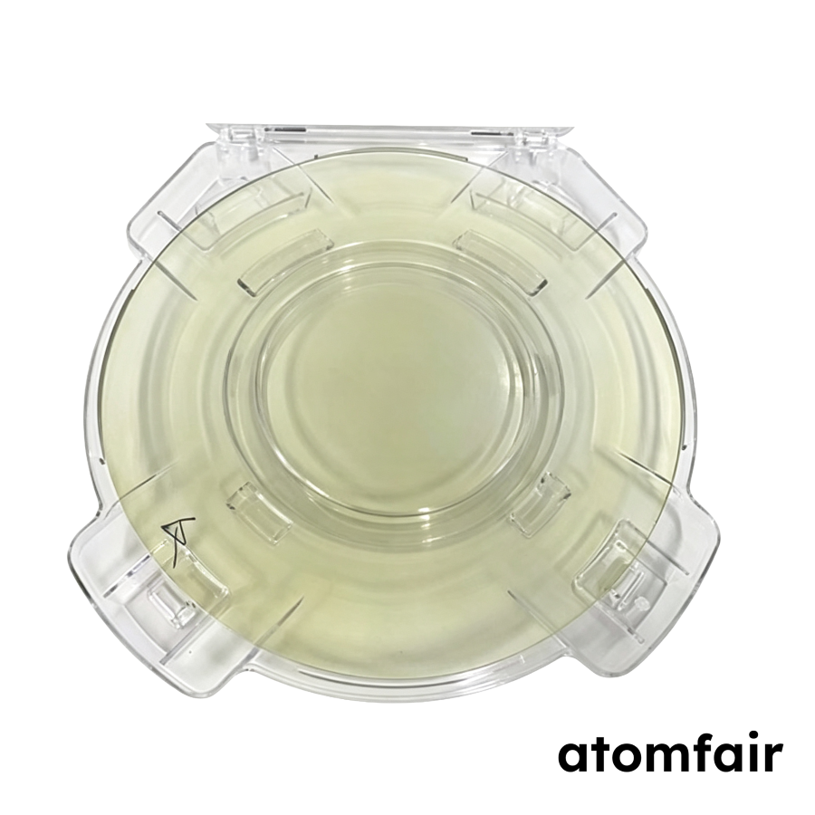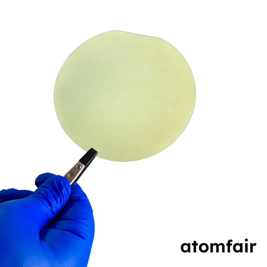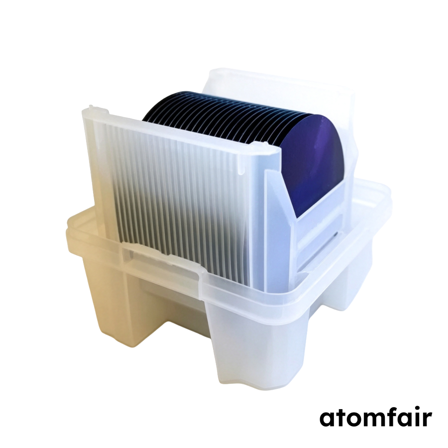
6 Inch Single-Side Oxidation Silicon Nitride WaferProduct Type: Silicon nitride wafer
Research-grade laboratory product
|
|||||||||||||||||||||||||||
|
|||||||||||||||||||||||||||
|
LABORATORY PROCUREMENT SUPPORT
For model selection, substrate matching or configuration confirmation, contact our technical sales team.
E-MAIL: inquiry@atomfair.com
|
|||||||||||||||||||||||||||
|
Supplier: Atomfair
Brand: ATOMFAIR®
|
Fabrication parameters including crystal orientation, SiO2 thickness, and processing route must be specified prior to manufacturing. Substrate matching, surface treatment, and integration requirements should be confirmed for compatibility.
- Crystal Orientation Specification: Crystal orientation must be selected from <100>, <111>, or <110> based on the intended application.
- SiO2 Film Thickness Confirmation: SiO2 film thickness must be confirmed within the 5 nm to 10 μm range, with conventional thickness between 100-500 nm.
- Processing Route Declaration: The processing route, either oxidation furnace or PECVD, must be stated for specification confirmation.
- Conductivity and Resistivity Bands: Conductivity type (N-type, P-type, or undoped high-resistivity) and target resistivity band must be specified.
- Substrate and Integration Compatibility: Substrate compatibility, surface treatment, and intended integration requirements should be confirmed before quotation.
What SiO2 film thickness options are available for the 6-inch single-side oxidation silicon nitride wafer?
The listed SiO2 film thickness range is 5 nm to 10 μm, with a conventional thickness of 100–500 nm. The exact thickness must be confirmed before quotation. Oxidation furnace and PECVD are the listed processing routes available for specification confirmation.
Which crystal orientation, conductivity type, and resistivity options can be specified for this Atomfair AF-SINX-6IN-S wafer?
Crystal orientation can be <100>, <111>, or <110>, and conductivity type can be N-type, P-type, or undoped high-resistivity. Resistivity bands are < 0.001 ohm.cm for heavily doped material, 1–100 ohm.cm for lightly doped material, and > 100–20000 ohm.cm for undoped material. Orientation, conductivity type, and target resistivity band must all be confirmed before quotation.
What compatibility and integration details must be confirmed before ordering this 6-inch single-side oxidation wafer?
Atomfair requires confirmation of the substrate, surface treatment, and intended integration requirements before quotation. You must also confirm the 6-inch size, single-side oxidation configuration, crystal orientation, SiO2 film thickness, conductivity type, target resistivity band, and the preferred oxidation furnace or PECVD processing route. These checks are required to align the wafer specification with the downstream process.
This 6-inch single-side oxidation silicon nitride wafer offers selectable crystal orientations (<100>, <111>, <110>), SiO2 film thickness from 5 nm to 10 μm, and conductivity types (N, P, undoped) with resistivity ranges from heavily doped <0.001 ohm·cm to undoped >10,000 ohm·cm, processed via oxidation furnace or PECVD. The broad parameter configurability supports diverse thin-film and device integration requirements, but the dependence on pre-quotation confirmation for all major specifications imposes a non-trivial procurement planning step for labs.
Positive
- Wide SiO2 thickness range: SiO2 film thickness from 5 nm to 10 μm, with conventional 100-500 nm, allows fine-tuning for gate dielectrics, passivation layers, or optical interference stacks in semiconductor or photonics integration.
- Multiple crystal orientations and doping: Availability of <100>, <111>, <110> orientations and N/P-type or undoped high-resistivity substrates supports epitaxial growth, MEMS processing, or tailored electrical isolation in advanced functional material research.
Trade-offs
- Specification confirmation required pre-order: Crystal orientation, SiO2 thickness, conductivity type, resistivity band, and processing route must all be confirmed before quotation, adding a mandatory engineering review step to procurement.
- Processing route dependency: Oxidation furnace versus PECVD routes yield different film stoichiometry and interface quality, and the customer must state the preferred method, requiring knowledge of deposition trade-offs for the intended lab application.
Every advanced material, component, equipment, and instrument in our catalog is backed by rigorous testing. We maintain strict internal quality management frameworks and align with CE conformity metrics to deliver transparent, reproducible performance data via our public open-science repository.
To request raw batch performance data, submit formal vendor registration paperwork, or execute a fast-turnaround R&D manufacturing loop, contact us at inquiry@atomfair.com.
Item is dispatched under the Atomfair Shipping & Delivery Framework (Free worldwide shipping on orders over $59 USD excl. heavy equipment). Return is governed by the Atomfair Return & Refund Policy (7-day technical return window).