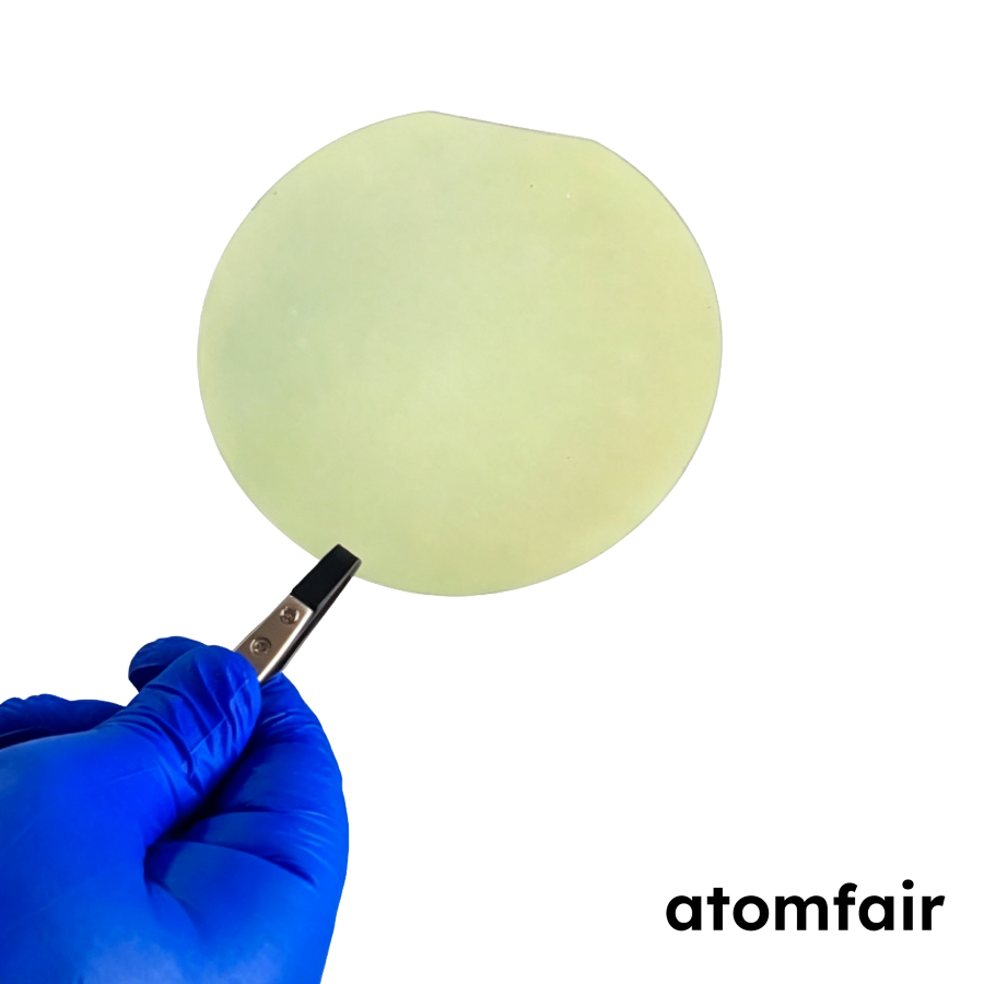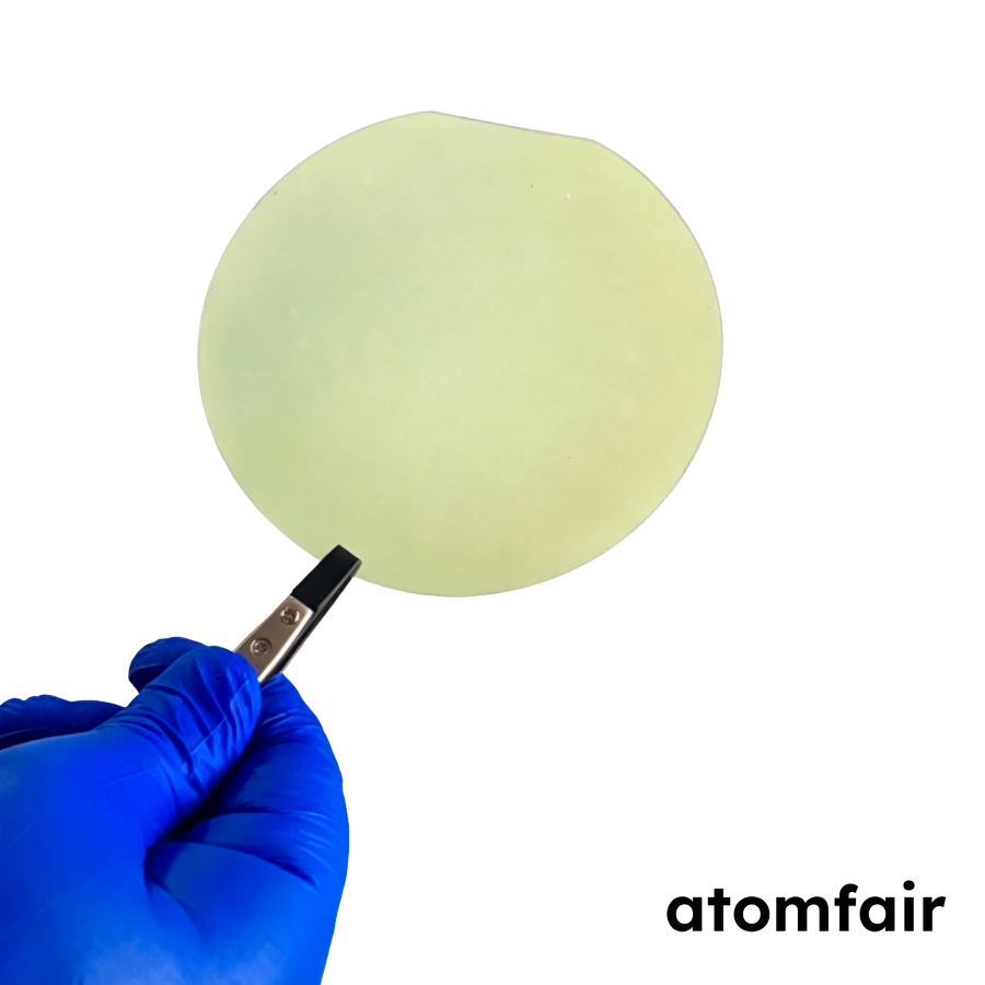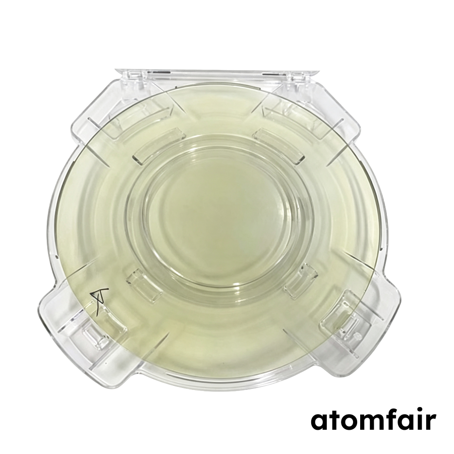
12 Inch Multilayer Continuous Film CVD MoS2 Thin Film on SiO2/Si SubstrateProduct Type: Multilayer Continuous Film
Research-grade laboratory product
|
|||||||||||||||||||||||||||||||
|
|||||||||||||||||||||||||||||||
|
LABORATORY PROCUREMENT SUPPORT
For model selection, substrate matching or configuration confirmation, contact our technical sales team.
E-MAIL: inquiry@atomfair.com
|
|||||||||||||||||||||||||||||||
|
Supplier: Atomfair
Brand: ATOMFAIR®
|
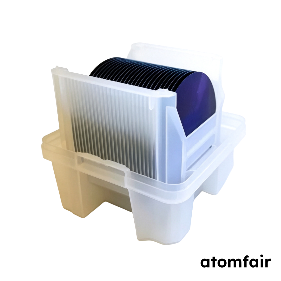
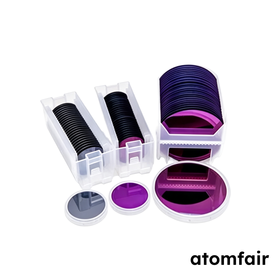
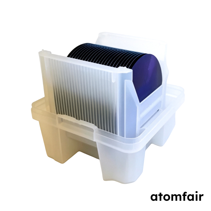
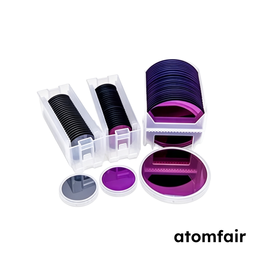
This CVD-grown MoS2 thin film is supplied on a SiO2/Si substrate with a 300 nm oxide layer. The film is compatible with transfer to PET, PI, ITO, FTO, glass, and metal substrates for diverse device integration.
- Transfer Compatibility: The multilayer continuous film can be transferred to specified alternative substrates, including PET, PI, ITO, FTO, glass, and metals.
What is the band gap of the multilayer MoS₂ film and how does it differ from monolayer MoS₂?
The multilayer continuous film MoS₂ has a bulk indirect band gap of approximately 1.23 eV, whereas monolayer MoS₂ exhibits a direct band gap of approximately 1.85 eV. This product is a multilayer film, so its band gap is indirect and near 1.23 eV, which influences its optical and electronic properties for near-infrared to visible applications.
Can the MoS₂ film be transferred to alternative substrates for flexible device integration?
Yes, the CVD-grown MoS₂ multilayer film is transfer-compatible to substrates including PET, PI, ITO, FTO, glass, and metal. This enables integration into flexible electronics, optoelectronics, and sensing devices by transferring the film from the growth SiO₂/Si substrate to the desired target substrate.
What is the typical grain size of the triangular single-crystal grains in the multilayer MoS₂ film?
The typical grain size of the triangular single-crystal grains is several tens to approximately one hundred micrometers per side. This grain size is characteristic of the CVD growth method and is a key parameter for device uniformity and performance in large-area applications.
This 12-inch multilayer continuous film CVD MoS2 on SiO2/Si (300 nm oxide) offers a large-area, undoped n-type layered semiconductor with a bulk indirect band gap of ~1.23 eV, suitable for scale-up in optoelectronic and sensing applications, but requires careful handling due to substrate fragility and transfer complexity.
Positive
- Large-area 12-inch continuous film: The 12-inch size enables wafer-scale integration for microelectronic and optoelectronic device fabrication, reducing edge effects and improving batch-to-batch uniformity compared to smaller substrates.
- Transfer-compatible substrate versatility: Compatibility with PET, PI, ITO, FTO, glass, and metal substrates allows the film to be post-process transferred for flexible or transparent electronics without compromising the CVD-grown quality.
Trade-offs
- Bulk indirect band gap limitation: The multilayer continuous film has an indirect band gap of ~1.23 eV, which reduces photoluminescence efficiency and limits suitability for direct-band-gap optoelectronic applications such as light-emitting diodes without exfoliation to monolayer.
- Handling and transfer complexity: The 12-inch SiO2/Si substrate is brittle and requires careful handling during transfer to alternative substrates; the process demands specialized wet or dry transfer techniques, increasing risk of film cracking or contamination.
Every advanced material, component, equipment, and instrument in our catalog is backed by rigorous testing. We maintain strict internal quality management frameworks and align with CE conformity metrics to deliver transparent, reproducible performance data via our public open-science repository.
To request raw batch performance data, submit formal vendor registration paperwork, or execute a fast-turnaround R&D manufacturing loop, contact us at inquiry@atomfair.com.
Item is dispatched under the Atomfair Shipping & Delivery Framework (Free worldwide shipping on orders over $59 USD excl. heavy equipment). Return is governed by the Atomfair Return & Refund Policy (7-day technical return window).