|
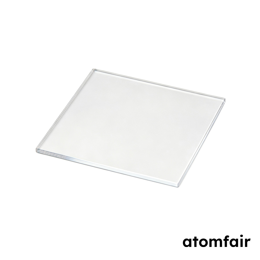
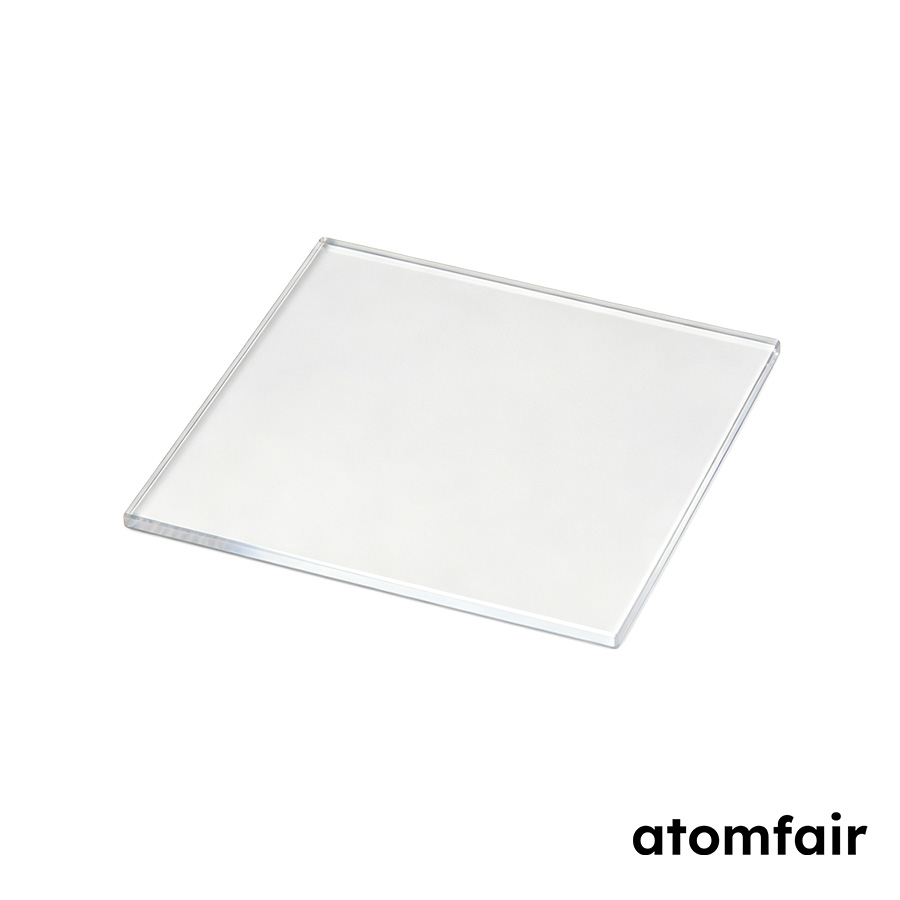
Quartz glass Substrate – 4 inch (100 mm), 25 pcs/box
Product Type: Glass substrate
Research-grade laboratory product
|
|||||||||||||||||||||||||||
|
|||||||||||||||||||||||||||
|
PRODUCT SELECTION SUPPORT
For model selection, material matching or specification support, contact our technical sales team.
E-MAIL: inquiry@atomfair.com
|
|||||||||||||||||||||||||||
|
Manufacturer: Atomfair LLC
Brand: ATOMFAIR®
|
The substrate surface quality of Scratch/Dig 40/20 and roughness Ra <0.5 nm require contamination-free handling to avoid defects. Flatness below 5 um necessitates careful mounting to prevent warping or stress-induced distortion.
- Surface Contamination Risk: Contact with bare skin or non-cleanroom gloves can deposit oils or particles that degrade the specified Scratch/Dig 40/20 surface quality.
- Mechanical Stress Sensitivity: Excessive clamping force or uneven support during processing may induce bowing that exceeds the <5 um flatness tolerance.
These steps ensure the substrate maintains its specified surface quality and flatness during unpacking and inspection. Use only cleanroom-grade tools and work surfaces to prevent contamination.
Required Equipment: Cleanroom-grade tweezers or vacuum wand, Lint-free cleanroom wipes, Particle-free compressed air or nitrogen gun
- Prepare Work Area
Set up a clean, static-dissipative work surface in a Class 100 or better cleanroom environment. - Inspect Packaging
Verify the box seal is intact and the substrates are separated by interleaving sheets to prevent scratching. - Remove Substrate
Grasp the substrate edge with cleanroom tweezers or a vacuum wand, avoiding contact with the front or back surfaces. - Clean Surface
Gently blow off any loose particles using particle-free compressed air at low pressure. - Inspect for Defects
Examine the substrate under bright, diffuse light for scratches, digs, or particulate contamination exceeding the 40/20 specification.
What is the significance of the 30 mm flat length on a 4-inch (100 mm) quartz substrate?
The 30 mm flat provides a primary orientation reference for alignment in semiconductor processing equipment. This standard flat length ensures compatibility with wafer handling systems that rely on a flat edge for rotational alignment, critical for photolithography and etching steps.
How does the ±25 µm thickness tolerance of the 500 µm quartz substrate impact thin-film deposition uniformity?
The thickness variation of ±25 µm can cause minor differences in thermal mass and capacitance across the substrate, potentially affecting the uniformity of deposited films in processes like PECVD or sputtering. For high-uniformity requirements, tighter thickness control may be necessary, but the specified tolerance is typical for standard research-grade substrates.
This 4-inch quartz glass substrate (AF-WF-S-GLAS-04IN-G073) offers a surface roughness of Ra <0.5 nm, flatness <5 µm, and Scratch/Dig 40/20 quality, making it suitable for demanding optical and thin-film applications where low scatter and precise substrate geometry are required.
Positive
- Ultra-low surface roughness: Ra <0.5 nm roughness minimizes optical scatter and provides a smooth foundation for thin-film deposition or photolithography.
- High surface quality specification: Scratch/Dig 40/20 ensures minimal surface defects, critical for high-precision optical and semiconductor processing.
Trade-offs
- Thin substrate handling required: At 500 ±25 µm thickness, the substrate is mechanically fragile and requires careful handling to avoid breakage during processing or transfer.
- Flatness constraint for large-area use: Flatness <5 µm may limit performance in applications requiring sub-micron planarity over the full 100 mm diameter, such as advanced lithography.
Every advanced material, component, equipment, and instrument in our catalog is backed by rigorous testing. We maintain strict internal quality management frameworks and align with CE conformity metrics to deliver transparent, reproducible performance data via our public open-science repository.
To request raw batch performance data, submit formal vendor registration paperwork, or execute a fast-turnaround R&D manufacturing loop, contact us at inquiry@atomfair.com.
Item is dispatched under the Atomfair Shipping & Delivery Framework (Free worldwide shipping on orders over $59 USD excl. heavy equipment). Return is governed by the Atomfair Return & Refund Policy (7-day technical return window).