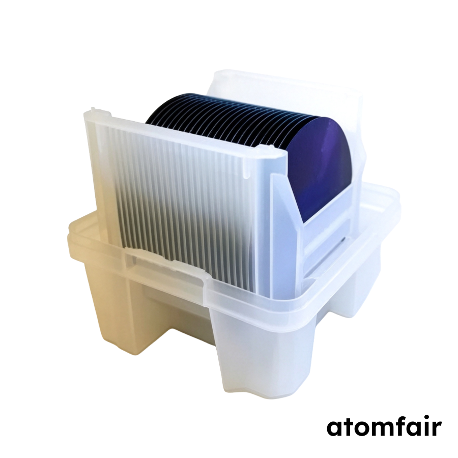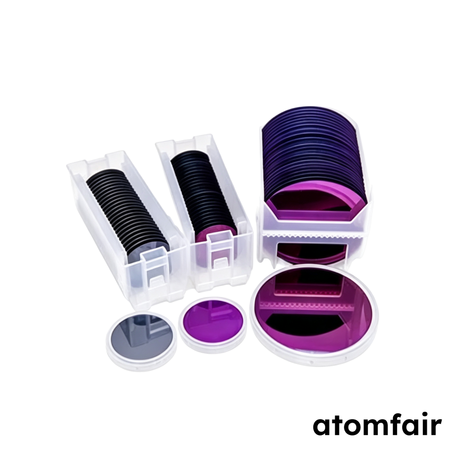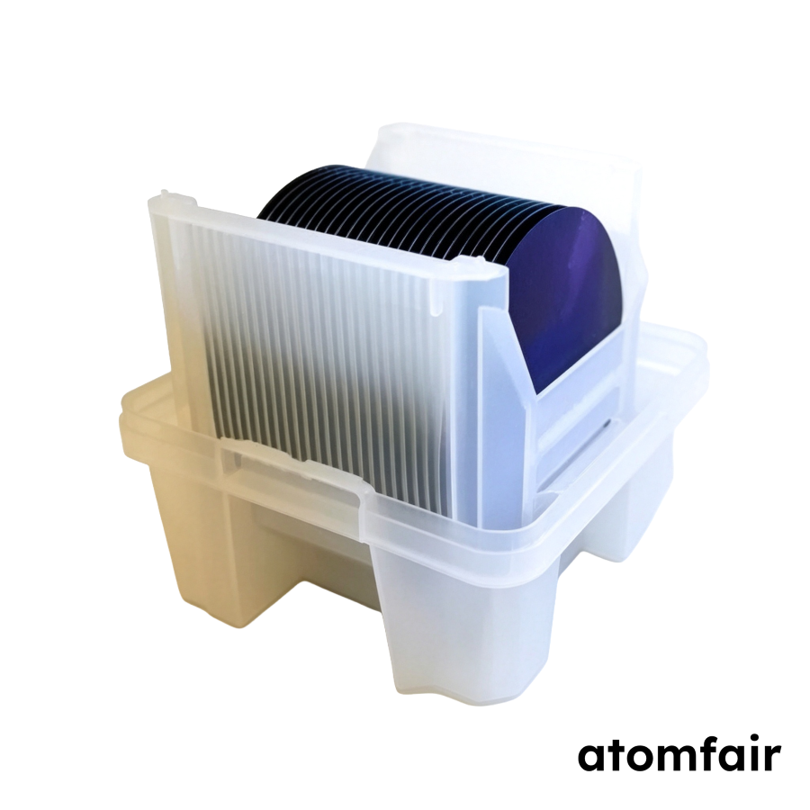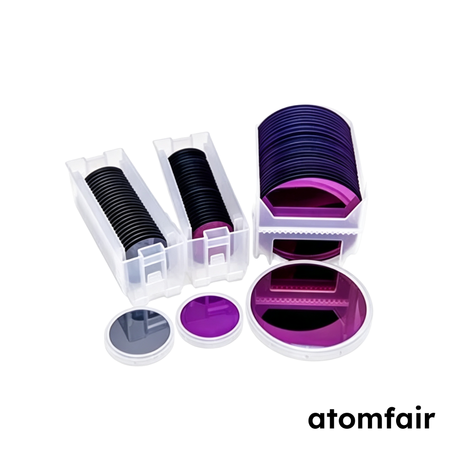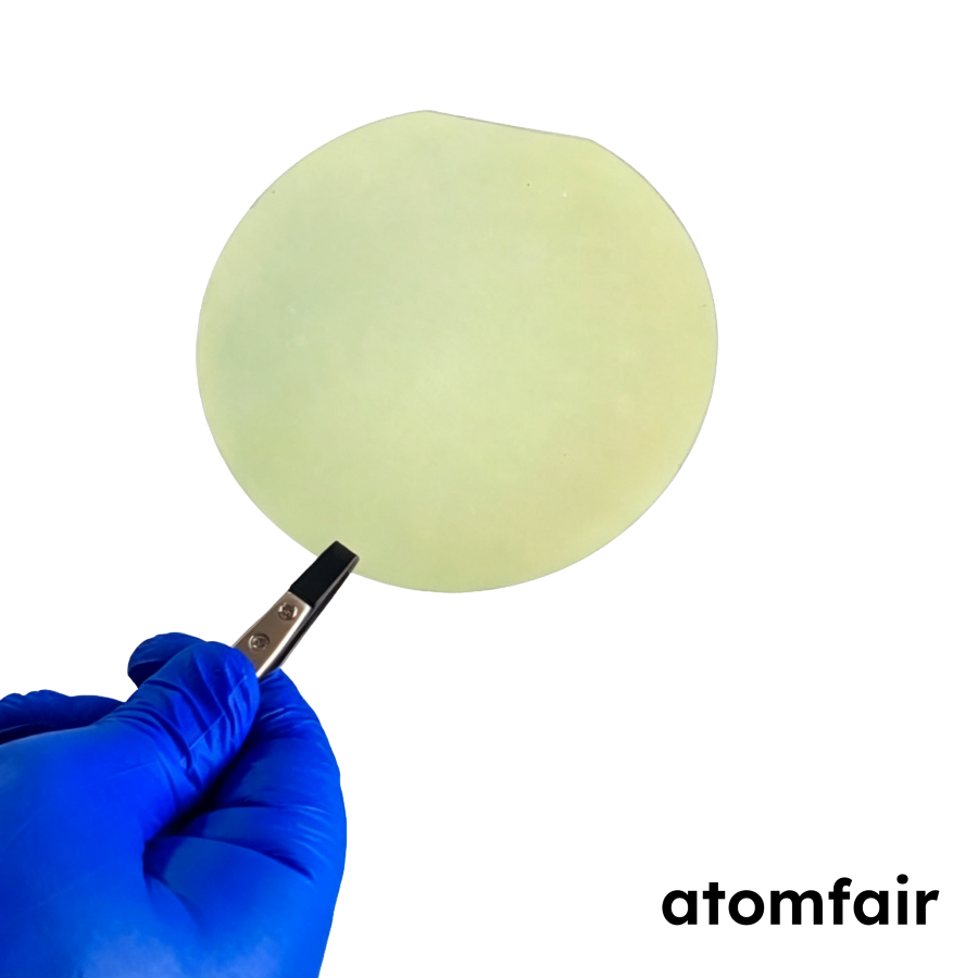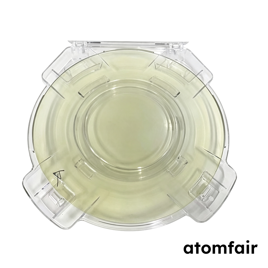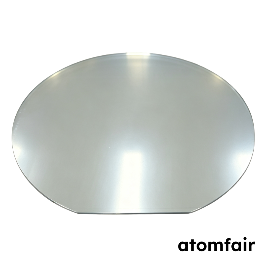
8 Inch Single-Sided Coating Platinum-Coated SubstrateProduct Type: Platinum-coated substrate
Research-grade laboratory product
|
|||||||||||||||||||||||||||||
|
|||||||||||||||||||||||||||||
|
LABORATORY PROCUREMENT SUPPORT
For model selection, substrate matching or configuration confirmation, contact our technical sales team.
E-MAIL: inquiry@atomfair.com
|
|||||||||||||||||||||||||||||
|
Supplier: Atomfair
Brand: ATOMFAIR®
|
This platinum-coated substrate requires confirmation of substrate type, surface treatment, and integration requirements before use. The coating process (electron-beam evaporation or magnetron sputtering) and substrate dimensions must be specified for proper handling and compatibility.
- Substrate Type Selection: Substrate must be selected from silicon, glass, quartz, or sapphire to match intended application requirements.
- Coating Process Compatibility: The film stack is deposited via electron-beam evaporation or magnetron sputtering, which require cleanroom or controlled environment conditions.
- Surface Roughness Constraint: The platinum coating maintains a surface roughness Ra ≤ 1 nm, which imposes strict cleanliness and handling protocols to avoid contamination.
- Film Purity Requirement: The film purity of ≥ 99.999% necessitates high-purity deposition conditions and substrate preparation to avoid contamination.
- Custom Dimension Verification: Substrate size, specification, and thickness can be customized and must be confirmed prior to quotation to ensure compatibility with deposition equipment.
Why does the 8-inch platinum-coated substrate include a 30 nm titanium adhesion layer beneath the 100 nm platinum layer?
The Ti 30 nm layer serves as an adhesion promoter between the substrate and the Pt 100 nm coating, ensuring mechanical stability and preventing delamination during subsequent processing or use. The film stack is specified as Ti 30 nm / Pt 100 nm, and the substrate can be silicon, glass, quartz, or sapphire, all of which benefit from the Ti adhesion layer.
What substrate materials are available for the 8-inch single-sided platinum-coated substrate, and how does substrate choice affect experimental compatibility?
The substrate can be silicon wafer, glass, quartz, or sapphire, with custom dimensions and thickness available. The substrate type influences thermal expansion, electrical conductivity, and optical transparency, so the choice should be matched to the specific experimental requirements such as high-temperature annealing or optical measurements.
Which coating process—electron-beam evaporation or magnetron sputtering—is recommended for this platinum-coated substrate, and what are the practical implications?
Both electron-beam evaporation and magnetron sputtering are available for the Ti 30 nm / Pt 100 nm film stack. Electron-beam evaporation typically yields higher film purity, while magnetron sputtering offers better step coverage and adhesion. The selection should be based on the intended application and the substrate's surface characteristics.
This 8-inch single-sided platinum-coated substrate offers a Ti 30 nm / Pt 100 nm film stack with Ra ≤ 1 nm roughness and ≥ 99.999% purity, deposited via electron-beam evaporation or magnetron sputtering on silicon, glass, quartz, or sapphire substrates, providing a versatile platform for high-precision electrode or contact layer applications.
Positive
- Ultra-Smooth Platinum Surface with High Purity: The stated Ra ≤ 1 nm roughness and ≥ 99.999% film purity enable consistent electrical contact and minimal scattering in surface-sensitive electrochemical or photonic applications.
- Substrate Material Flexibility: Availability of silicon, glass, quartz, or sapphire substrates allows users to match thermal expansion, optical transparency, or dielectric properties to experimental or device requirements.
Trade-offs
- Custom Specifications Require Pre-Order Confirmation: Substrate type, thickness, and exact dimensions must be confirmed before quotation, introducing lead time and requiring precise specification at order placement.
- 8-Inch Size Imposes Handling and Integration Constraints: The 8-inch diameter limits compatibility with smaller sample mounts or chamber geometries, and the large area increases risk of film non-uniformity across the substrate if not carefully processed.
Every advanced material, component, equipment, and instrument in our catalog is backed by rigorous testing. We maintain strict internal quality management frameworks and align with CE conformity metrics to deliver transparent, reproducible performance data via our public open-science repository.
To request raw batch performance data, submit formal vendor registration paperwork, or execute a fast-turnaround R&D manufacturing loop, contact us at inquiry@atomfair.com.
Item is dispatched under the Atomfair Shipping & Delivery Framework (Free worldwide shipping on orders over $59 USD excl. heavy equipment). Return is governed by the Atomfair Return & Refund Policy (7-day technical return window).