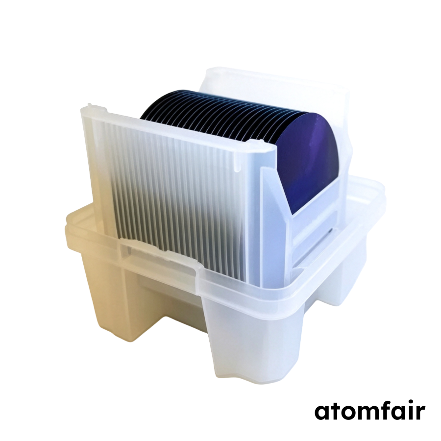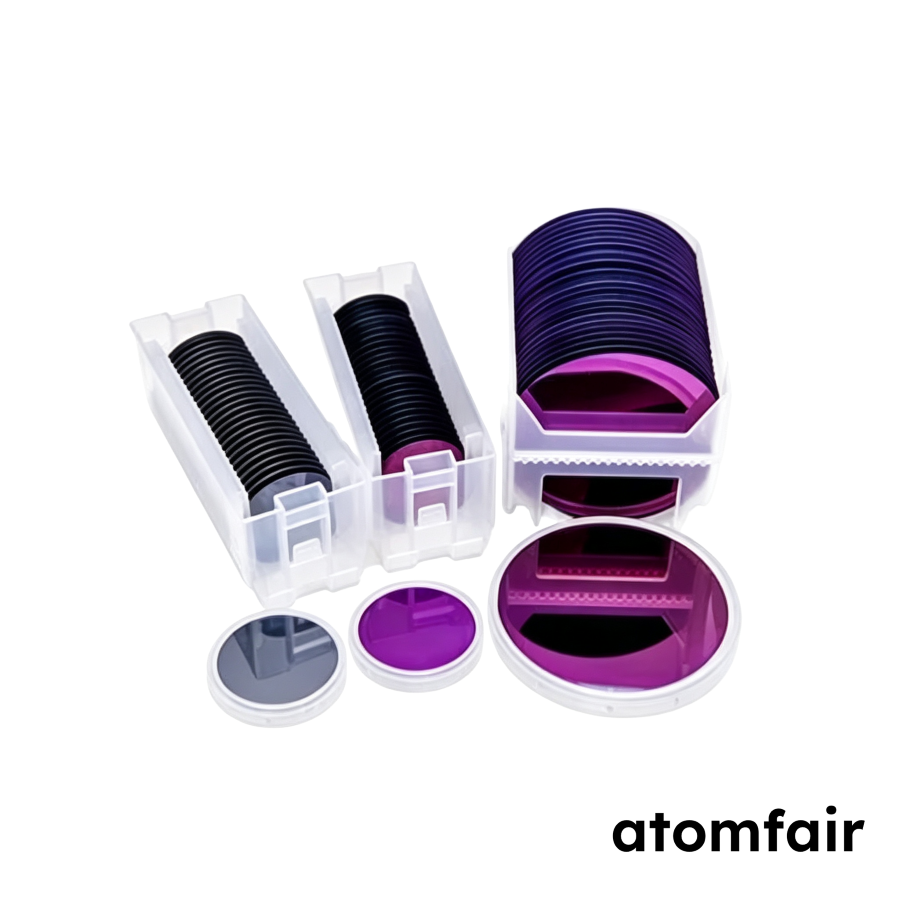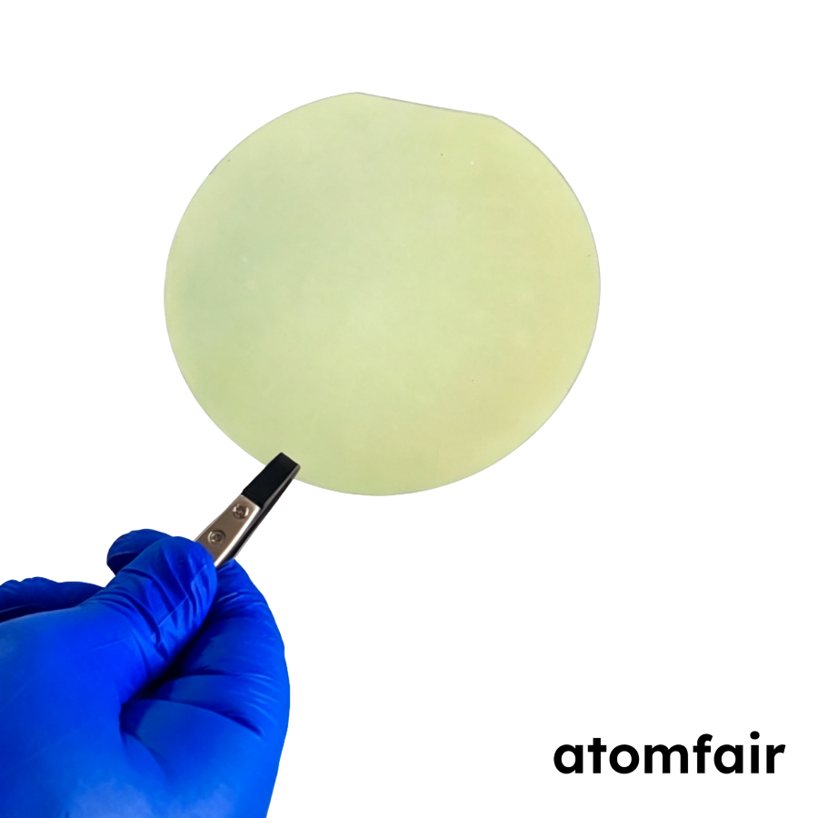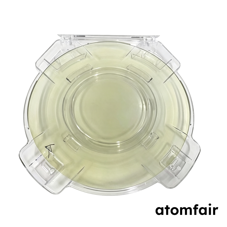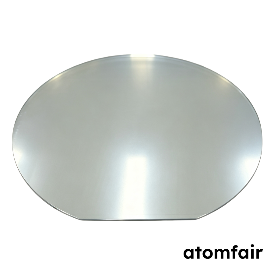
2 Inch Double-Sided Coating Platinum-Coated SubstrateProduct Type: Platinum-coated substrate
Research-grade laboratory product
|
|||||||||||||||||||||||||||||
|
|||||||||||||||||||||||||||||
|
LABORATORY PROCUREMENT SUPPORT
For model selection, substrate matching or configuration confirmation, contact our technical sales team.
E-MAIL: inquiry@atomfair.com
|
|||||||||||||||||||||||||||||
|
Supplier: Atomfair
Brand: ATOMFAIR®
|
What surface roughness and film purity are specified for the 2 inch double-sided platinum-coated substrate?
The listed specification is Ra ≤ 1 nm surface roughness and film purity ≥ 99.999%. These values apply to the Ti 30 nm / Pt 100 nm double-sided coating on the selected substrate, which can be silicon, glass, quartz, or sapphire.
Which substrate materials and deposition processes are compatible with Atomfair's 2 inch Pt-coated substrate?
The substrate can be a silicon wafer, glass, quartz, or sapphire, and the coating can be produced by electron-beam evaporation or magnetron sputtering. Substrate dimensions, specification, and thickness are customizable, but the substrate type and coating process must be confirmed before quotation.
What order details must be confirmed before Atomfair will quote this 2 inch double-sided Pt-coated substrate?
Confirmation is required for the 2 inch size, double-sided coating, Ti 30 nm / Pt 100 nm film stack, substrate type, substrate thickness, and coating process. Custom dimensions and specifications should be included in the quotation request.
The 2-inch double-sided Pt-coated substrate (Ti 30 nm / Pt 100 nm) offers a high-purity (≥99.999%), low-roughness (Ra ≤1 nm) working surface on multiple substrate options, but the Ti adhesion layer and film stack may impose thermal or chemical processing limits in aggressive CVD or high-temperature anneal steps.
Positive
- Ultra-smooth, high-purity Pt surface: Film roughness Ra ≤1 nm and purity ≥99.999% provide a clean, uniform working surface suitable for sensitive electrochemical or thin-film device applications.
- Multi-substrate flexibility: Available on silicon, glass, quartz, or sapphire, allowing the user to match thermal expansion and optical transparency to the experimental or device stack requirements.
Trade-offs
- Ti adhesion layer thermal limit: The 30 nm titanium interlayer may interdiffuse or form silicides at elevated process temperatures, restricting anneal or deposition conditions depending on substrate choice.
- Coating process confirmation needed: The substrate type, thickness, and coating process (e-beam vs. sputtering) must be confirmed before quotation, and these choices influence film stress, adhesion, and compatibility with downstream processing.
Every advanced material, component, equipment, and instrument in our catalog is backed by rigorous testing. We maintain strict internal quality management frameworks and align with CE conformity metrics to deliver transparent, reproducible performance data via our public open-science repository.
To request raw batch performance data, submit formal vendor registration paperwork, or execute a fast-turnaround R&D manufacturing loop, contact us at inquiry@atomfair.com.
Item is dispatched under the Atomfair Shipping & Delivery Framework (Free worldwide shipping on orders over $59 USD excl. heavy equipment). Return is governed by the Atomfair Return & Refund Policy (7-day technical return window).