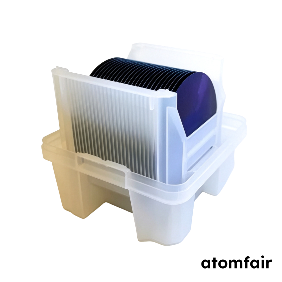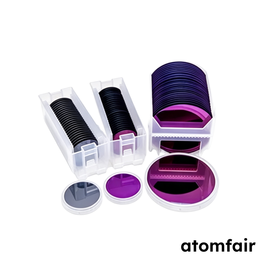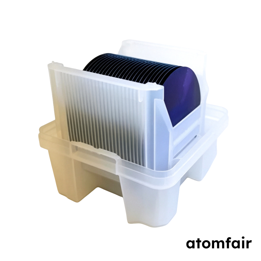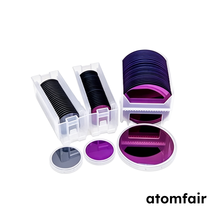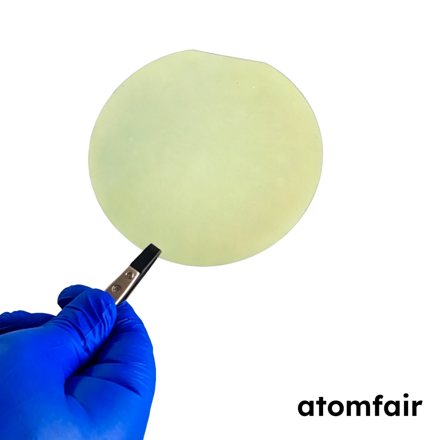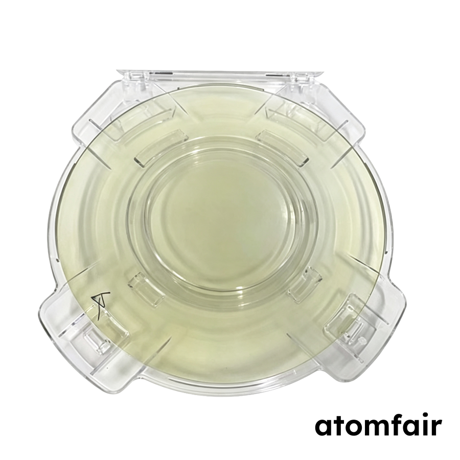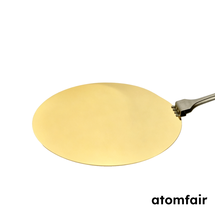
6 Inch Double-Sided Coating Gold-Coated SubstrateProduct Type: Gold-coated substrate
Research-grade laboratory product
|
|||||||||||||||||||||||||||||
|
|||||||||||||||||||||||||||||
|
LABORATORY PROCUREMENT SUPPORT
For model selection, substrate matching or configuration confirmation, contact our technical sales team.
E-MAIL: inquiry@atomfair.com
|
|||||||||||||||||||||||||||||
|
Supplier: Atomfair
Brand: ATOMFAIR®
|
What is the role of the chromium adhesion layer in the Au film stack on this gold-coated substrate?
The Cr 30 nm layer acts as an adhesion promoter between the substrate and the Au 100 nm layer, preventing delamination and ensuring long-term film stability. This specific film stack is a standard architecture for enhancing gold adhesion to substrates such as silicon, glass, quartz, or sapphire.
Which substrate material should be selected for high-temperature or high-vacuum applications?
For high-temperature and high-vacuum environments, quartz or sapphire are preferred due to their low outgassing and thermal stability. The product offers substrate options including silicon, glass, quartz, and sapphire, with customization available for thickness and dimensions.
What surface roughness specification is guaranteed and why is it critical for this gold-coated substrate?
The product guarantees a surface roughness of Ra < 1 nm, which is critical for minimizing scattering losses in optical and plasmonic devices. This specification, combined with a film purity of ≥ 99.999%, ensures high reflectivity and low defect density for demanding research applications.
This 6-inch double-sided gold-coated substrate with a Cr 30 nm / Au 100 nm film stack is evaluated for its ultra-smooth (Ra < 1 nm) and high-purity (≥99.999%) coating, suitable for precision optical and electronic applications, though users must confirm substrate type, thickness, and coating process prior to quotation.
Positive
- Ultra-smooth and high-purity coating: The film roughness is specified as Ra < 1 nm with a purity of ≥99.999%, providing a high-quality surface for demanding applications such as reflectometry or plasmonics.
- Flexible substrate and process options: Supports silicon wafer, glass, quartz, or sapphire substrates, with electron-beam evaporation or magnetron sputtering as available coating routes, enabling adaptation to different experimental requirements.
Trade-offs
- Custom configuration requires pre-order confirmation: Substrate type, thickness, and coating process must be confirmed before quotation, introducing lead time and requiring detailed specification input from the buyer.
- Limited to single film stack specification: The listed Cr 30 nm / Au 100 nm stack is fixed unless customized, and the double-sided coating adds complexity for handling in processes requiring single-sided access only.
Every advanced material, component, equipment, and instrument in our catalog is backed by rigorous testing. We maintain strict internal quality management frameworks and align with CE conformity metrics to deliver transparent, reproducible performance data via our public open-science repository.
To request raw batch performance data, submit formal vendor registration paperwork, or execute a fast-turnaround R&D manufacturing loop, contact us at inquiry@atomfair.com.
Item is dispatched under the Atomfair Shipping & Delivery Framework (Free worldwide shipping on orders over $59 USD excl. heavy equipment). Return is governed by the Atomfair Return & Refund Policy (7-day technical return window).