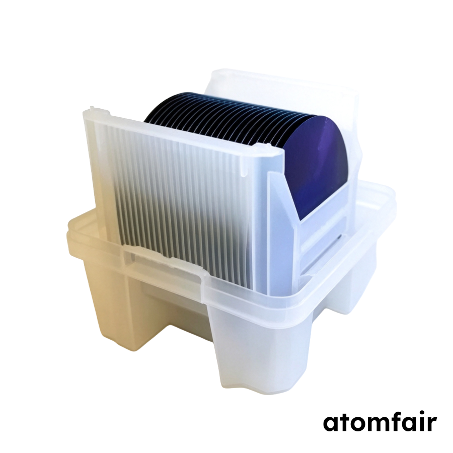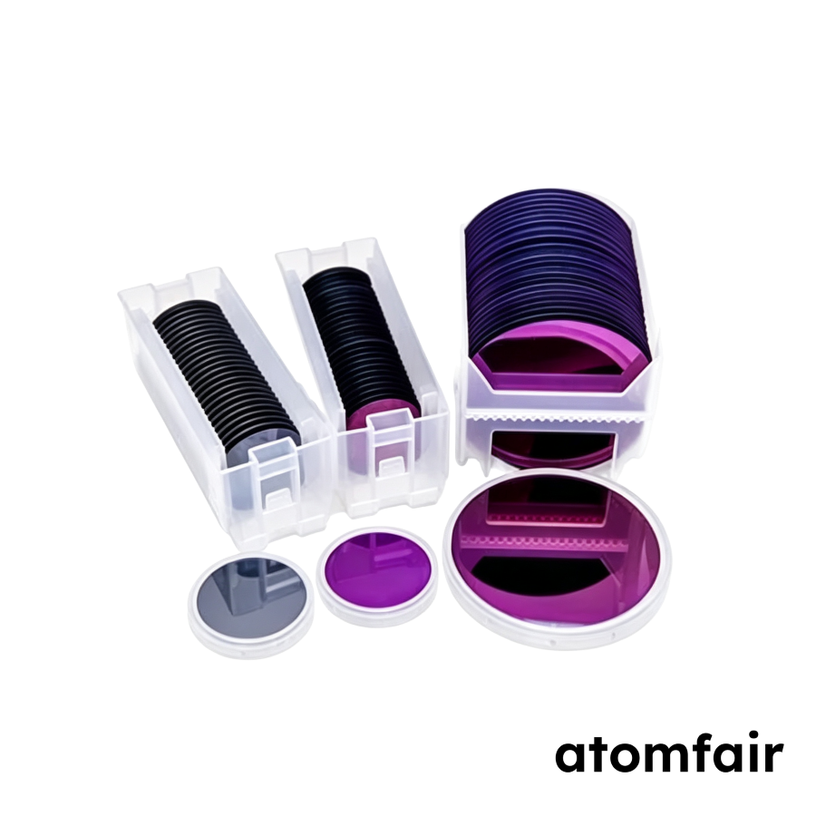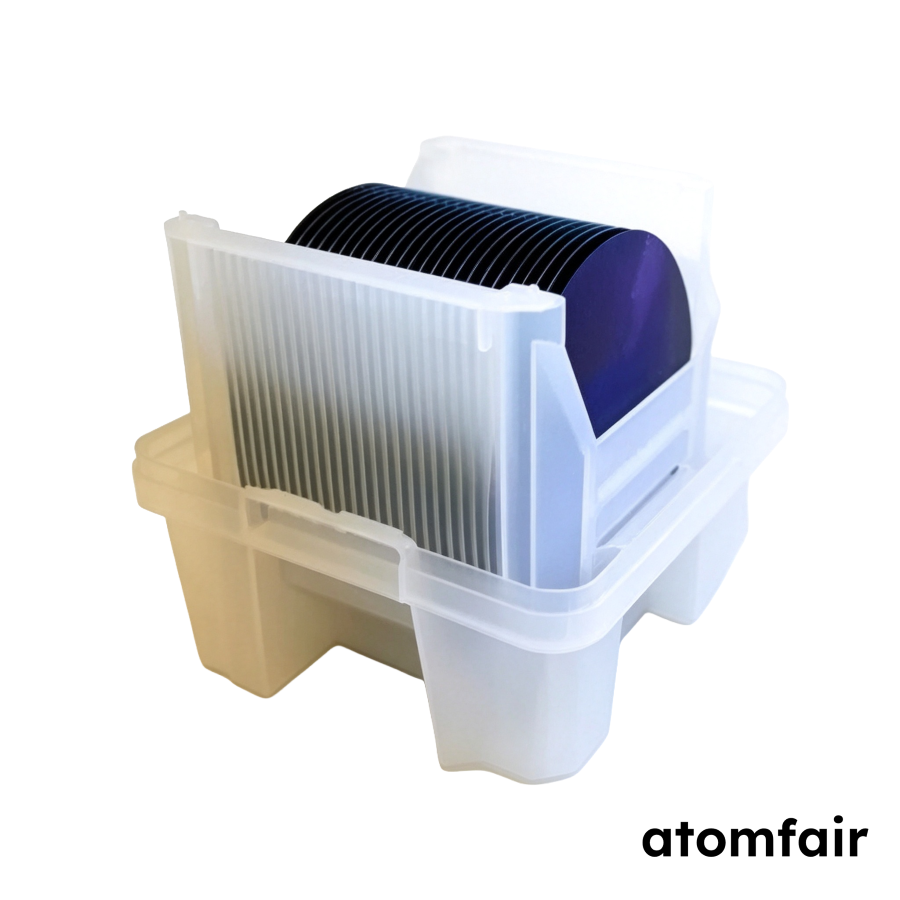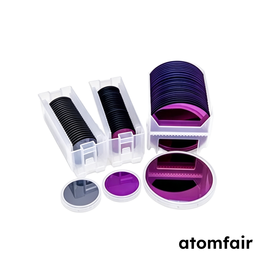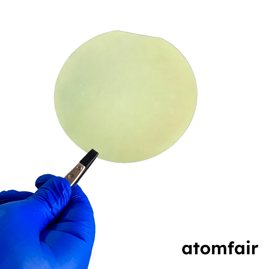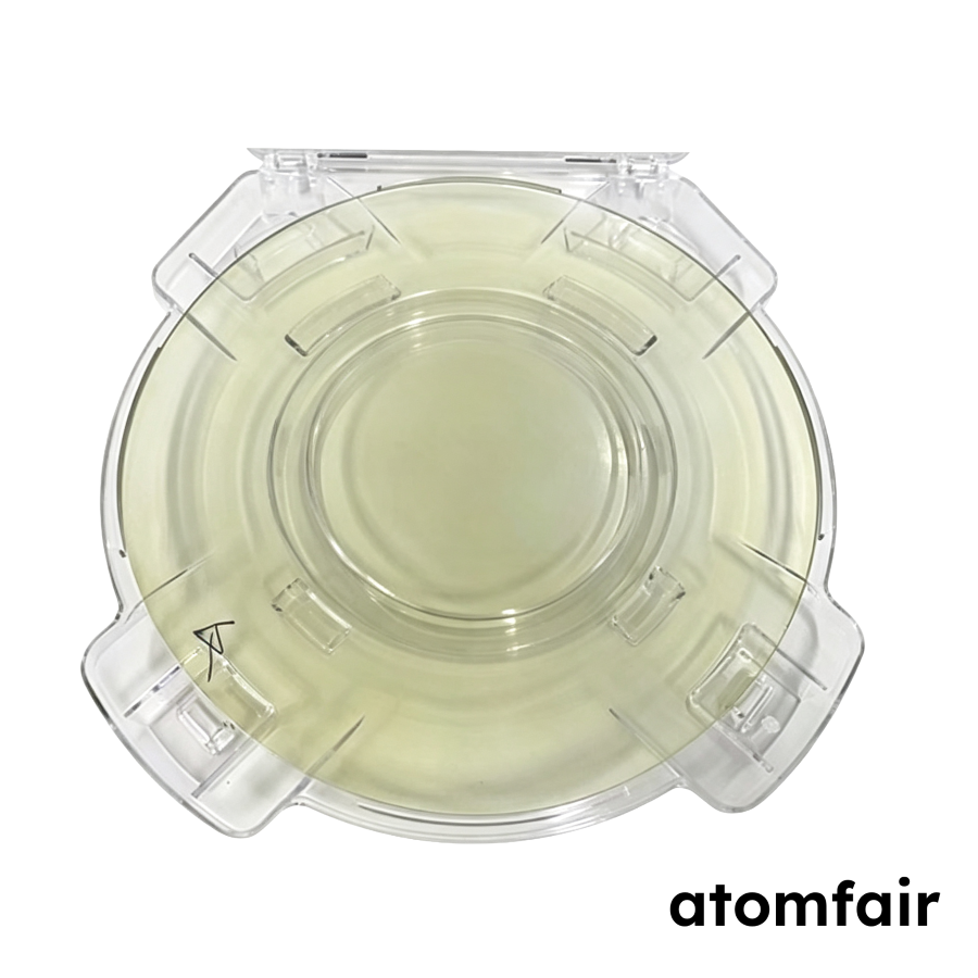
4 Inch Single-Layer Continuous Film CVD MoS2 Thin Film on SiO2/Si SubstrateProduct Type: Single-Layer Continuous Film
Research-grade laboratory product
|
|||||||||||||||||||||||||||||||
|
|||||||||||||||||||||||||||||||
|
LABORATORY PROCUREMENT SUPPORT
For model selection, substrate matching or configuration confirmation, contact our technical sales team.
E-MAIL: inquiry@atomfair.com
|
|||||||||||||||||||||||||||||||
|
Supplier: Atomfair
Brand: ATOMFAIR®
|
This single-layer continuous MoS2 film is supplied on a SiO2/Si carrier and must be handled as an integration-ready research material rather than a standalone device. Transfer compatibility is limited to PET, PI, ITO, FTO, glass, and metal substrates, so substrate selection and surface treatment must be confirmed before processing.
- Substrate compatibility: Confirm that the final substrate is limited to PET, PI, ITO, FTO, glass, or metal before initiating a transfer because the product listing specifies only these transfer-compatible substrate classes.
- Surface treatment and integration confirmation: Confirm the required surface treatment and intended integration route before processing because these requirements determine whether the selected substrate configuration is compatible.
- Application-specific handling: Use handling and transfer procedures suited to the intended optoelectronic, microelectronic, biosensing, or chemical sensing application, as the product is listed for these device fields.
- Mechanical support: Keep the film on the supplied SiO2/Si substrate until transfer because the single-layer continuous film is not free-standing and requires the carrier for mechanical support.
What is the direct band gap of monolayer MoS2 and how does it enable optoelectronic applications?
The monolayer MoS2 film has a direct band gap of approximately 1.85 eV, as stated in the technical specifications. This direct band gap allows efficient photon emission and absorption, making it suitable for optoelectronic devices such as photodetectors and light-emitting diodes. In contrast, bulk MoS2 has an indirect band gap of 1.23 eV, which is less efficient for light-based applications.
Can this MoS2 film be transferred onto flexible substrates like PET?
Yes, the film is transfer-compatible. The product description lists PET, PI, ITO, FTO, glass, and metal substrates as compatible transfer targets. The as-grown film on SiO2/Si can be transferred to these substrates using established transfer techniques, enabling integration into flexible or transparent devices.
What is the typical grain size of the single-layer MoS2 film and why is it important?
The typical grain size of the triangular single-crystal grains is several tens to approximately one hundred micrometers per side, as per the specification. Grain size influences device performance because larger grains reduce grain boundary density, which can lead to higher carrier mobility and lower scattering in microelectronic and optoelectronic devices.
This 4-inch single-layer continuous film CVD MoS2 on SiO2/Si with 300 nm oxide provides a direct band gap of ~1.85 eV suitable for optoelectronic and microelectronic device R&D, but the undoped n-type nature and CVD process impose strict handling and integration constraints.
Positive
- Direct band gap at monolayer: The monolayer exhibits a direct band gap of approximately 1.85 eV, enabling efficient photon absorption and emission for optoelectronic and photonic device applications.
- Transfer-compatible substrate flexibility: The film can be transferred to PET, PI, ITO, FTO, glass, or metal substrates, allowing integration with diverse device architectures and flexible electronics platforms.
Trade-offs
- Undoped n-type semiconductor: The undoped MoS2 layer is intrinsically n-type, which may limit p-type device integration or require additional doping steps for complementary logic or junction devices.
- Transfer process dependency: The film is supplied on SiO2/Si and requires wet or dry transfer for alternate substrates, introducing risks of mechanical damage or contamination during handling.
Every advanced material, component, equipment, and instrument in our catalog is backed by rigorous testing. We maintain strict internal quality management frameworks and align with CE conformity metrics to deliver transparent, reproducible performance data via our public open-science repository.
To request raw batch performance data, submit formal vendor registration paperwork, or execute a fast-turnaround R&D manufacturing loop, contact us at inquiry@atomfair.com.
Item is dispatched under the Atomfair Shipping & Delivery Framework (Free worldwide shipping on orders over $59 USD excl. heavy equipment). Return is governed by the Atomfair Return & Refund Policy (7-day technical return window).