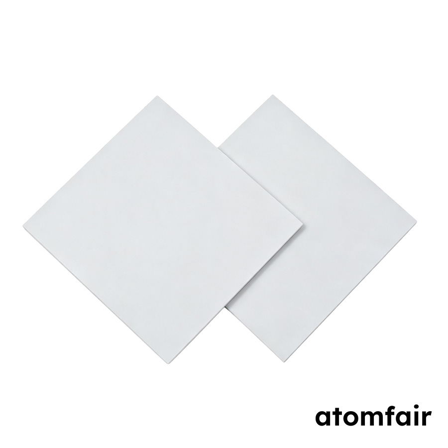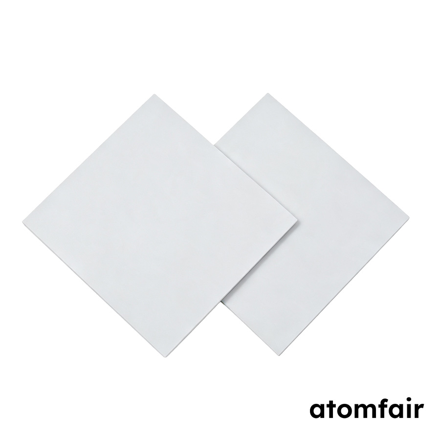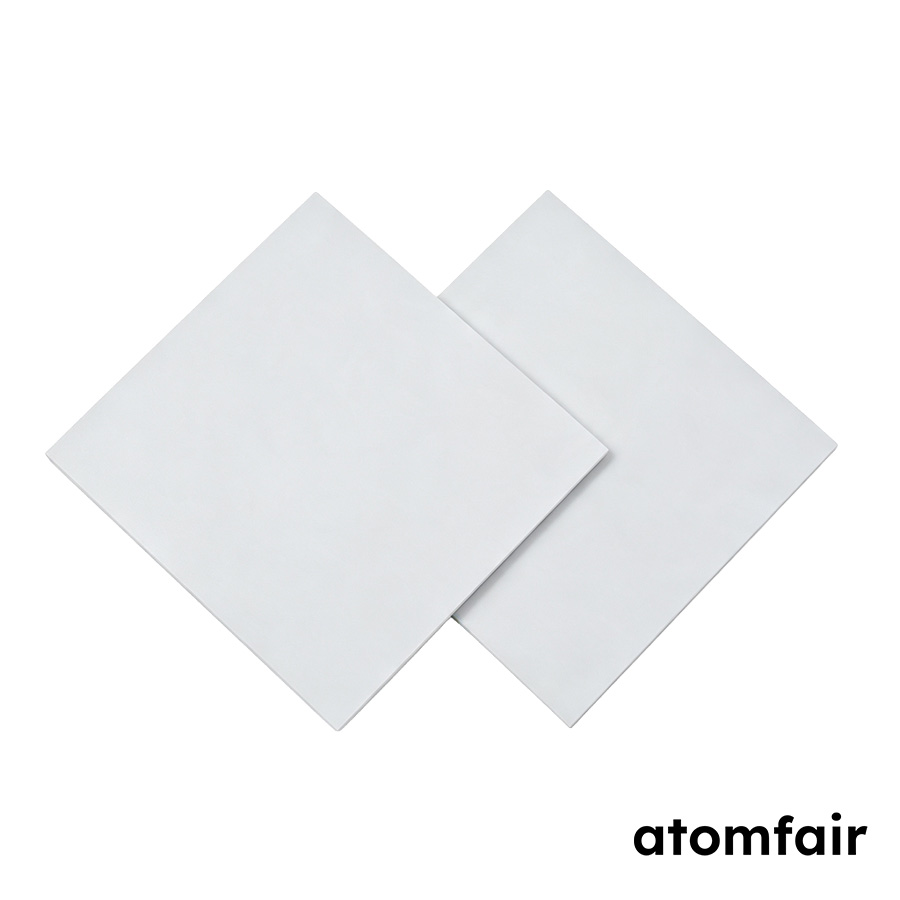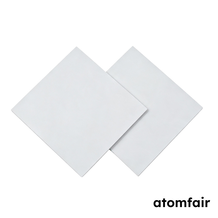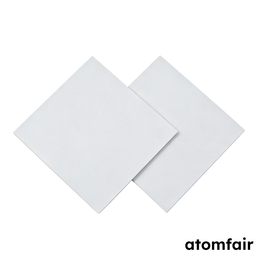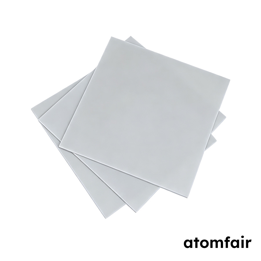
Aluminum Nitride Ceramic Substrate, 10 mm x 10 mm x 1 mm, Pack of 10Product Type: Technical ceramic substrate
Research-grade laboratory product
|
|||||||||||||||||||||||||||||||||
|
|||||||||||||||||||||||||||||||||
|
LABORATORY PROCUREMENT SUPPORT
For model selection, accessory matching, platform compatibility or configuration confirmation, contact our technical sales team.
E-MAIL: inquiry@atomfair.com
|
|||||||||||||||||||||||||||||||||
|
Supplier: Atomfair
Brand: ATOMFAIR®
|
How does the Young's modulus of 320 GPa and fracture toughness of 3.0 MPa√m affect the mechanical reliability of this aluminum nitride substrate under thermal cycling?
The high Young's modulus provides excellent dimensional stability, but the moderate fracture toughness of 3.0 MPa√m indicates limited resistance to crack propagation. This trade-off is critical for thermal cycling applications where thermal stresses can initiate cracks, so the substrate's thermal expansion match to silicon helps mitigate stress.
Why is the thermal expansion coefficient of this aluminum nitride substrate matched to silicon, and how does it benefit power module assembly?
The thermal expansion of aluminum nitride is close to that of silicon, which reduces thermal stress during soldering and operation. This compatibility improves the reliability of power modules and electronic component workflows, as stated in the product description.
What handling precautions are needed for this aluminum nitride substrate given its Vickers hardness of 11 GPa and surface roughness of 0.2-0.3 μm?
The substrate's high hardness (11 GPa) makes it resistant to scratching but also brittle, requiring careful handling to avoid chipping. The fine surface finish (Ra 0.2-0.3 μm) should be protected from contamination. For custom shapes or metallization, the manufacturer recommends confirming requirements before quotation.
Aluminum nitride ceramic substrate (10x10x1 mm, pack of 10) evaluated for high-power thermal management: thermal conductivity >170 W/(m·K) enables 7–10× improvement over alumina, but the 0.2–0.3 μm as-fired surface roughness and 15 kV/mm dielectric breakdown impose handling and voltage derating constraints in thin-film or high-field applications.
Positive
- High thermal conductivity >170 W/(m·K): Thermal conductivity is approximately 7–10 times higher than alumina ceramic, enabling effective heat spreading in power modules and high-brightness LED assemblies without active cooling.
- CTE matched to silicon: Coefficient of thermal expansion close to silicon reduces thermomechanical stress during solder reflow and power cycling, improving reliability of direct-bonded electronic components.
Trade-offs
- As-fired surface roughness of 0.2–0.3 μm: Surface roughness Ra of 0.2–0.3 μm limits direct thin-film metallization adhesion and may require post-processing polishing for fine-line circuit patterning.
- Dielectric breakdown strength ≥15 kV/mm: DC breakdown voltage of ≥15 kV/mm imposes a per-millimeter voltage standoff ceiling; users must consider operating voltage and substrate thickness trade-offs for high-field isolation.
Every advanced material, component, equipment, and instrument in our catalog is backed by rigorous testing. We maintain strict internal quality management frameworks and align with CE conformity metrics to deliver transparent, reproducible performance data via our public open-science repository.
To request raw batch performance data, submit formal vendor registration paperwork, or execute a fast-turnaround R&D manufacturing loop, contact us at inquiry@atomfair.com.
Item is dispatched under the Atomfair Shipping & Delivery Framework (Free worldwide shipping on orders over $59 USD excl. heavy equipment). Return is governed by the Atomfair Return & Refund Policy (7-day technical return window).