|
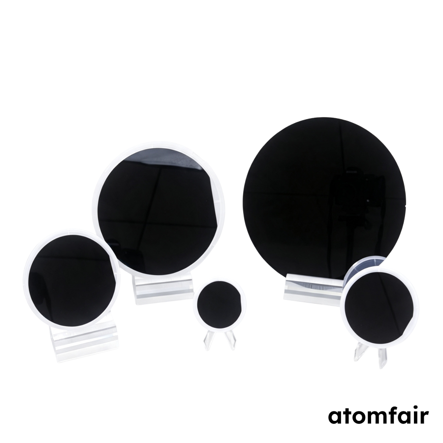
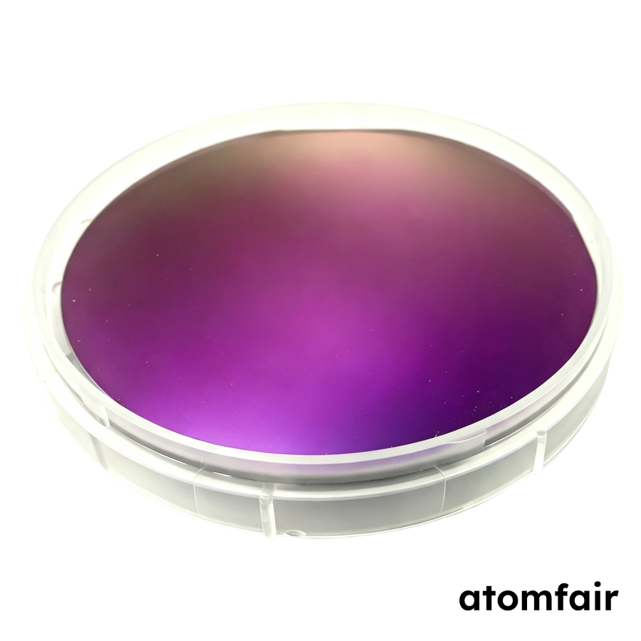
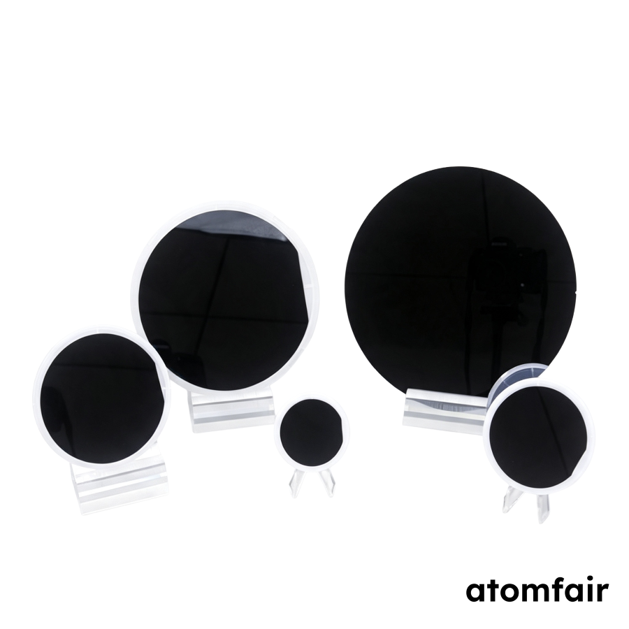
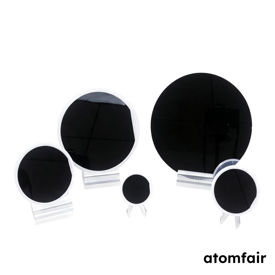
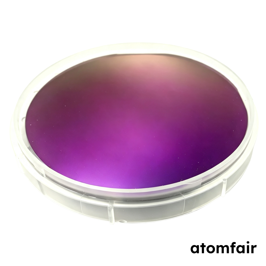
Thermal Oxidation Silicon Wafer – 2 inch (50.8 mm) Single-Side Polished, Single-sided oxidation 285 nm
Product Type: Thermal oxidation silicon wafer
Research-grade laboratory product
|
|||||||||||||||||||||||
|
|||||||||||||||||||||||
|
PRODUCT SELECTION SUPPORT
For model selection, material matching or specification support, contact our technical sales team.
E-MAIL: inquiry@atomfair.com
|
|||||||||||||||||||||||
|
Manufacturer: Atomfair LLC
Brand: ATOMFAIR®
|
The oxide layer is susceptible to contamination and mechanical damage from particulate exposure or improper handling. Environmental moisture and temperature fluctuations may affect oxide integrity over extended storage periods.
- Contamination Control: Store wafers in a cleanroom environment or sealed container to prevent particulate deposition on the oxide surface.
- Mechanical Protection: Handle wafers only at the edges using clean tweezers or vacuum wand to avoid scratching or delaminating the oxide layer.
Proper handling and cleaning procedures are critical to preserve oxide layer integrity before deposition or lithography. The following steps outline safe unpacking, inspection, and pre-processing preparation.
Required Equipment: Cleanroom gloves, Flat-tip tweezers or vacuum wand, Wafer carrier or cleanroom-grade container
- Inspect packaging for damage
Inspect the wafer shipping container for any signs of crushing or moisture ingress before opening. - Don cleanroom gloves
Don cleanroom gloves and ensure the work surface is clean and free of debris. - Remove wafer from container
Remove the wafer from its container by grasping the edge with flat-tip tweezers or a vacuum wand, avoiding contact with the polished or oxidized surfaces. - Inspect oxide surface
Inspect the oxide surface under a bright light for visible scratches, particles, or discoloration. - Transfer wafer to carrier
Transfer the wafer to a clean carrier or directly into the processing tool, ensuring the oxide side faces upward if single-side processing is required.
What oxide thickness options are available beyond the standard 285 nm?
In addition to the standard 285 nm oxide thickness, this thermal oxidation silicon wafer supports a customized range of 20–2000 nm. For orders outside the standard 285 nm, the desired thickness must be specified at the time of quotation. The product page lists 20–2000 nm as the available customization range, and technical sales can be contacted for specific thickness requirements.
What does single-sided oxidation mean for this thermal oxidation silicon wafer?
Single-sided oxidation means the silicon dioxide layer is grown only on one side of the wafer; the opposite side remains bare silicon. This is specified in the product as 'single-sided oxidation' with an oxide thickness of 285 nm. It is typically used in applications where electrical isolation or a dielectric layer is required on only one surface, such as in certain MEMS or sensor device fabrication processes.
What is the surface finish of this wafer?
This wafer is single-side polished (SSP), meaning one side is mirror-polished to a smooth finish suitable for photolithography and device patterning, while the other side is left unpolished (matte). The polish specification is explicitly listed as 'Single-Side Polished' in the technical specifications. This is a standard configuration for many semiconductor and research applications where only one side requires high surface quality.
This 2-inch thermal oxidation silicon wafer offers a single-sided 285 nm oxide layer on a 6N monocrystalline silicon substrate with a single-side polished finish, suitable for research applications requiring precise oxide thickness control and customization up to 2000 nm.
Positive
- Customizable oxide thickness range: Standard 285 nm oxide thickness is complemented by a 20–2000 nm customization range, allowing adaptation to application-specific dielectric or passivation requirements.
- High-purity monocrystalline silicon base: 6N (99.9999%) purity CZ or FZ silicon provides low defect density and consistent electronic properties critical for reliable device fabrication and experimental reproducibility.
Trade-offs
- Single-sided oxidation only: Oxide layer is applied to one side only, constraining use to asymmetric device designs and requiring additional processing for double-sided oxide applications.
- Single-side polished finish: Only one side is polished; the unpolished backside may introduce scattering or adhesion issues in optical or lithographic processes requiring a smooth double-sided surface.
Every advanced material, component, equipment, and instrument in our catalog is backed by rigorous testing. We maintain strict internal quality management frameworks and align with CE conformity metrics to deliver transparent, reproducible performance data via our public open-science repository.
To request raw batch performance data, submit formal vendor registration paperwork, or execute a fast-turnaround R&D manufacturing loop, contact us at inquiry@atomfair.com.
Item is dispatched under the Atomfair Shipping & Delivery Framework (Free worldwide shipping on orders over $59 USD excl. heavy equipment). Return is governed by the Atomfair Return & Refund Policy (7-day technical return window).