|
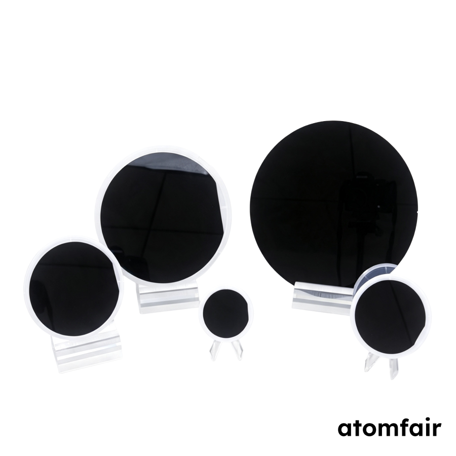
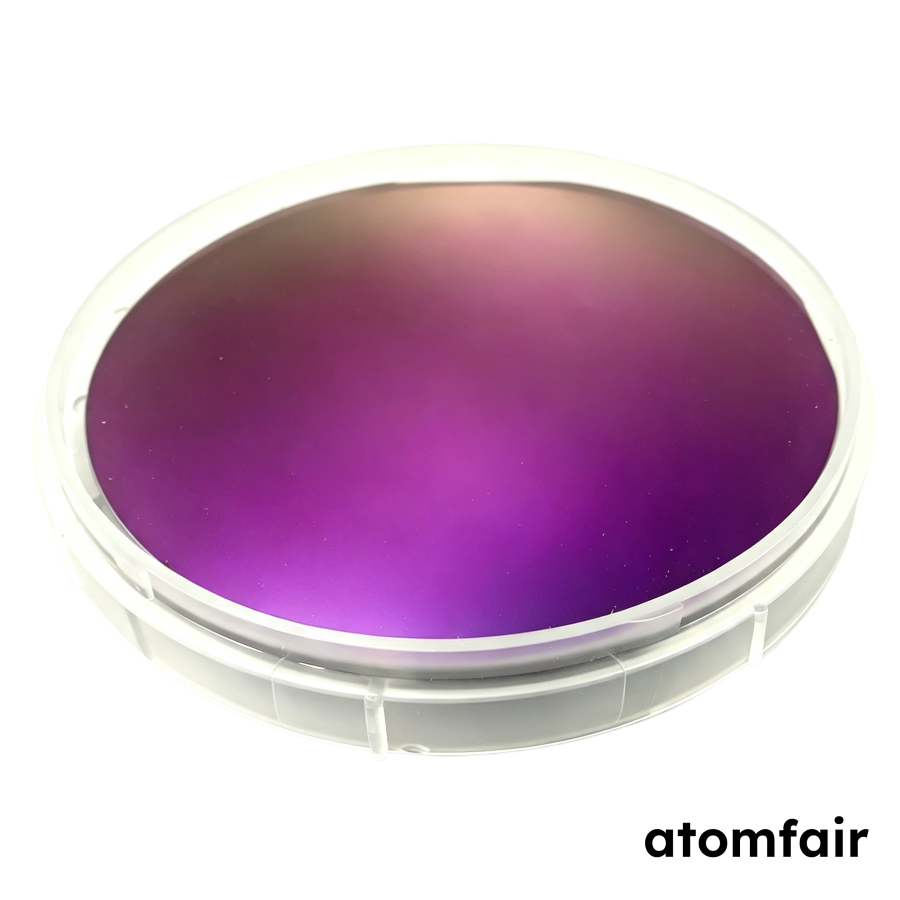
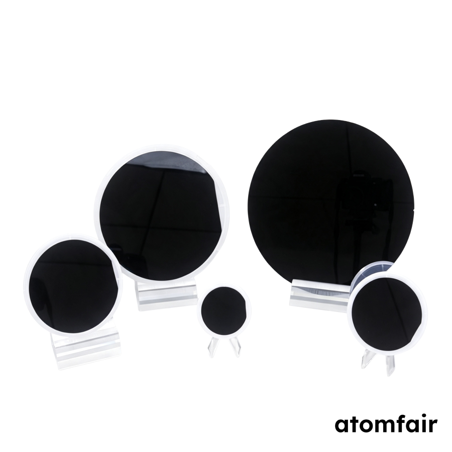
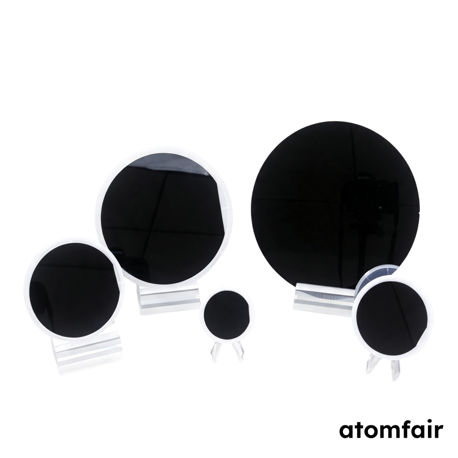
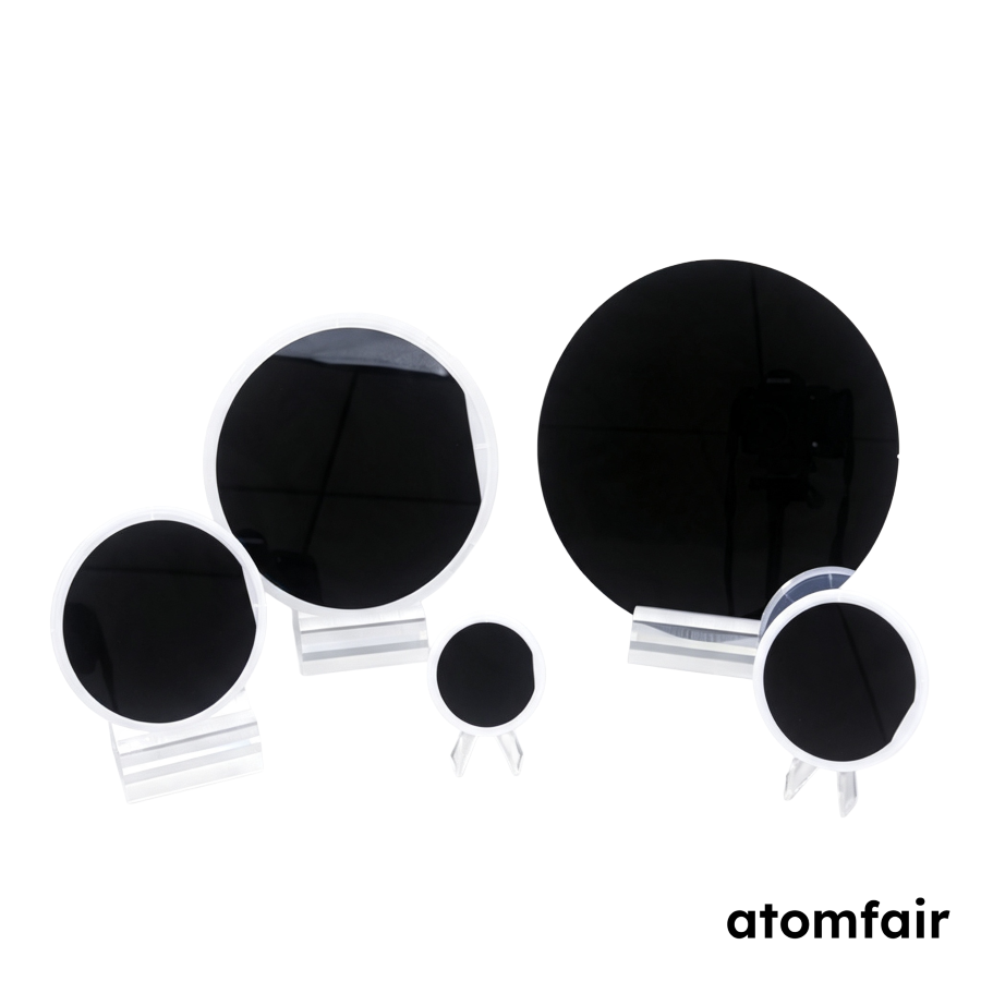
P type Monocrystalline Silicon Wafer – 4 inch (100 mm) <100> Double-Side Polished
Product Type: Silicon wafer
Research-grade laboratory product
|
|||||||||||||||||||||||||||||||||||
|
|||||||||||||||||||||||||||||||||||
|
PRODUCT SELECTION SUPPORT
For model selection, material matching or specification support, contact our technical sales team.
E-MAIL: inquiry@atomfair.com
|
|||||||||||||||||||||||||||||||||||
|
Manufacturer: Atomfair LLC
Brand: ATOMFAIR®
|
What resistivity ranges are available for this 4-inch double-side polished P-type silicon wafer and how does resistivity impact device performance?
Available resistivity values include 0.001-0.005 ohm.cm, 1-10 ohm.cm, >10 ohm.cm, >5K ohm.cm, and >10K ohm.cm. The appropriate resistivity is selected based on the target device's doping requirements, as it directly influences carrier concentration, threshold voltage, and series resistance.
What are the flatness tolerances (TTV, BOW, WARP) of this 4-inch silicon wafer and why are they important for photolithography alignment?
The wafer has TTV <10 µm, BOW <10 µm, and WARP <15 µm. These tight tolerances are critical for maintaining uniform focus across the wafer during photolithography, reducing overlay errors and improving device yield.
Is this double-side polished silicon wafer suitable for both front-side and back-side processing?
Yes, the wafer is double-side polished with front-side roughness Ra <0.5 nm and back side roughness also Ra <0.5 nm, making it suitable for processes requiring high-quality surfaces on both sides, such as MEMS or power device fabrication.
This 4-inch P-type <100> monocrystalline silicon wafer with double-side polished surfaces offers tight geometric tolerances (TTV <10 µm, BOW <10 µm, WARP <15 µm) and surface roughness below 0.5 nm, making it suitable for high-precision device fabrication. The fixed 4-inch diameter and P-type doping should be considered for equipment compatibility and application requirements.
Positive
- Double-side polished with Ra <0.5 nm: Both front and back surfaces are polished to a roughness below 0.5 nm, enabling high-quality interfaces for epitaxy or bonding.
- Tight geometry tolerances: TTV <10 µm, BOW <10 µm, and WARP <15 µm ensure consistent device performance across the wafer.
Trade-offs
- Fixed 4-inch diameter: This wafer is supplied as a 4-inch (100 mm) diameter, which may limit compatibility with processing equipment designed for larger or non-standard wafer sizes.
- P-type doping only: The wafer is specified as P-type, restricting its use to applications that require p-type silicon; n-type is not available in this configuration.
Every advanced material, component, equipment, and instrument in our catalog is backed by rigorous testing. We maintain strict internal quality management frameworks and align with CE conformity metrics to deliver transparent, reproducible performance data via our public open-science repository.
To request raw batch performance data, submit formal vendor registration paperwork, or execute a fast-turnaround R&D manufacturing loop, contact us at inquiry@atomfair.com.
Item is dispatched under the Atomfair Shipping & Delivery Framework (Free worldwide shipping on orders over $59 USD excl. heavy equipment). Return is governed by the Atomfair Return & Refund Policy (7-day technical return window).