|
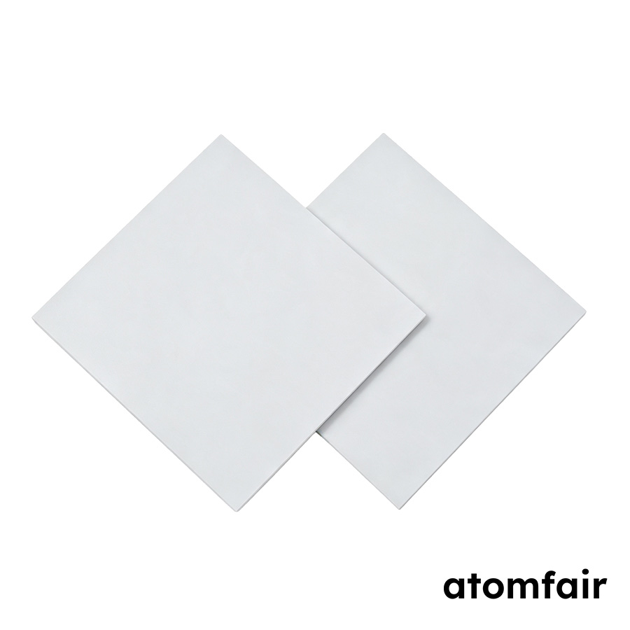
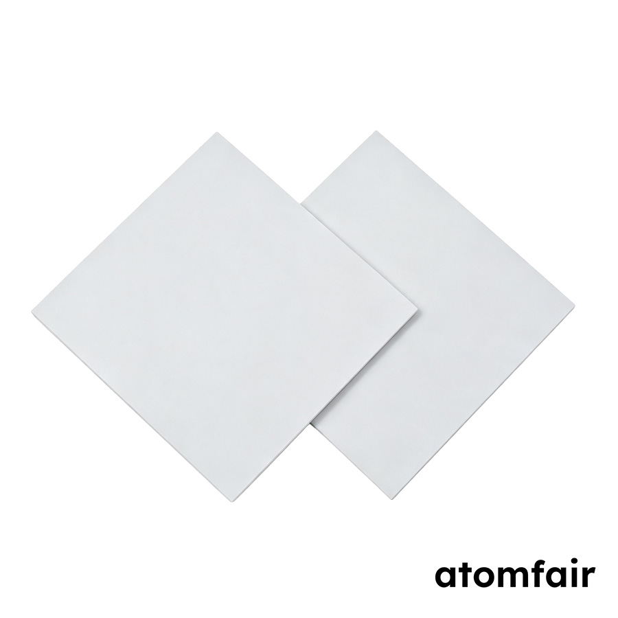
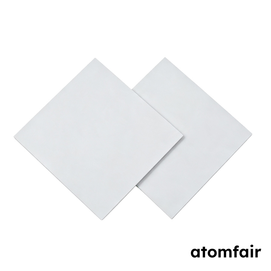
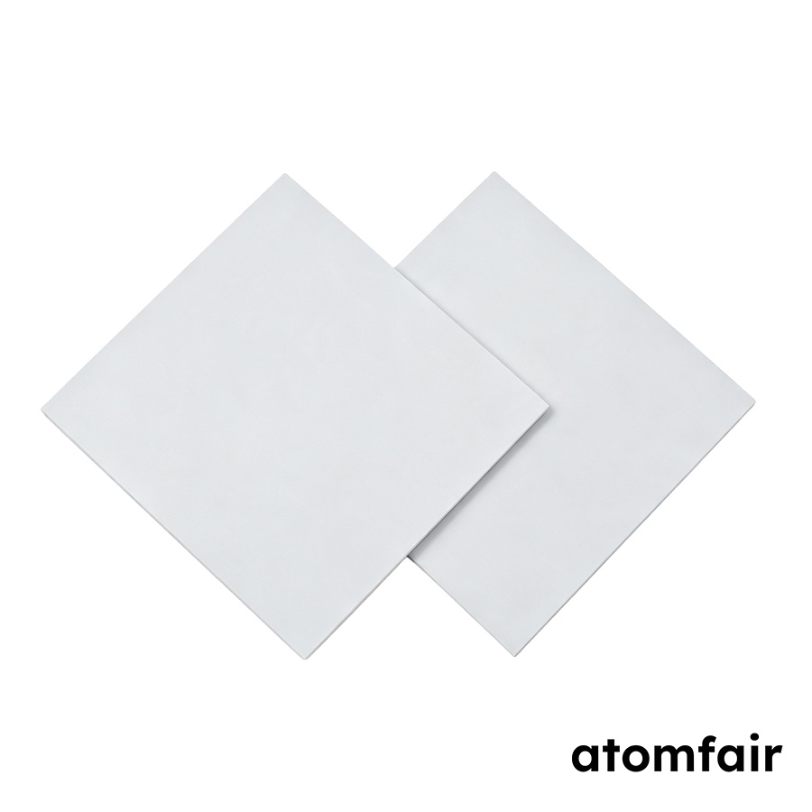
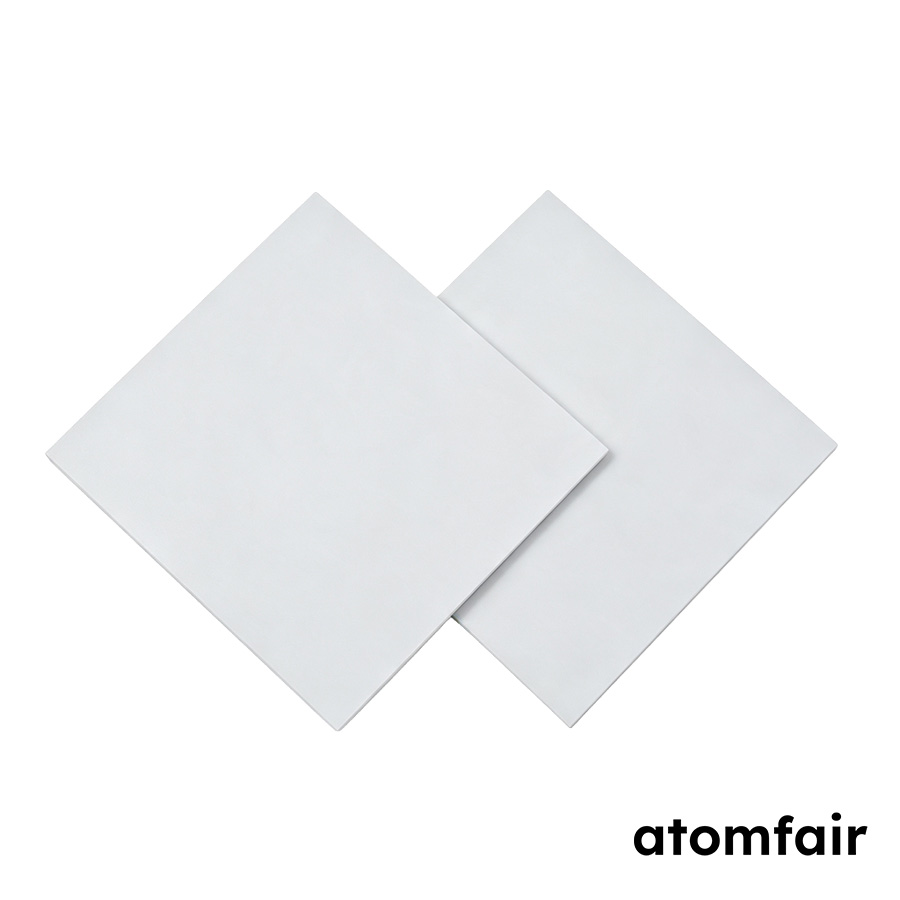
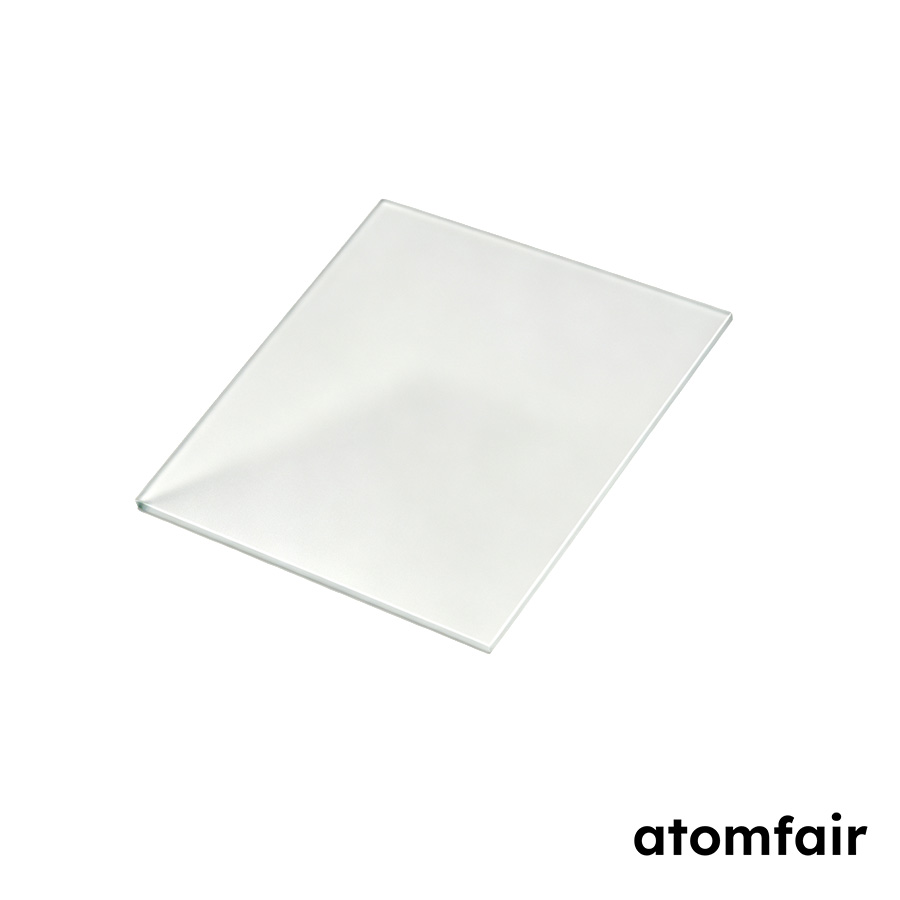
Yttria-Stabilized Zirconia Single Crystal Substrate, (110), DSP (10 pcs/box)
Product Type: YSZ single crystal substrate
Research-grade laboratory product
|
|||||||||||||||||||||||||||||||||||||||||||||||
|
|||||||||||||||||||||||||||||||||||||||||||||||
|
LABORATORY PROCUREMENT SUPPORT
For material matching, specification review, model selection or configuration confirmation, contact our technical sales team.
E-MAIL: inquiry@atomfair.com
|
|||||||||||||||||||||||||||||||||||||||||||||||
|
Manufacturer: Atomfair LLC
Brand: ATOMFAIR®
|
The YSZ substrate requires material matching to the target thin-film or device workflow. All specification parameters including orientation, dimensions, and polishing condition must be confirmed before ordering.
- Material Matching: Confirm that the substrate material and crystal family match the target thin-film or device workflow before quotation.
- Specification Review: Verify orientation, dimensions, thickness, polishing condition, offcut details, quantity, and any custom requirements for the selected option.
- Orientation Tolerance: Ensure the orientation tolerance of ±0.5° is acceptable for the intended deposition or analysis application.
- Surface Roughness: The surface roughness of <5 Å must be considered for thin-film growth or interface quality requirements.
This procedure outlines the steps to verify material compatibility and confirm all specifications before ordering. Following these steps ensures the substrate meets the requirements of the intended thin-film or device workflow.
- Match Material
Confirm that the YSZ substrate material and crystal family match the target thin-film or device workflow. - Review Specifications
Verify the orientation, dimensions, thickness, polishing condition, offcut details, quantity, and any custom requirements for the selected option. - Include Quotation Details
Include the selected specification option and required quantity when contacting Atomfair for quotation.
What is the orientation tolerance and surface roughness specification for the YSZ (110) single crystal substrate?
The orientation tolerance is ±0.5°, and the surface roughness is less than 5Å. These parameters are directly stated in the technical specifications and are critical for ensuring epitaxial film quality and minimizing defects in thin-film growth on the (110) plane.
What is the thermal expansion coefficient of the YSZ (110) substrate, and why is it important for high-temperature applications?
The thermal expansion coefficient is 10.3 × 10⁻⁶ /°C, as listed in the specifications. This value is important for matching with materials that will be processed or operated at elevated temperatures, reducing thermal stress and delamination risk during deposition or annealing.
What is the crystal structure and lattice constant of the YSZ (110) substrate, and how does it influence lattice matching?
The YSZ substrate has a cubic crystal structure with a lattice constant of 5.125 Å, as specified. This parameter is essential for assessing lattice mismatch with target thin-film materials, which is critical for minimizing dislocations and ensuring high-quality epitaxy on the (110) orientation.
This YSZ (110) single crystal substrate offers a high melting point of 2800°C and ultra-smooth surface roughness below 5 Å, suitable for high-temperature epitaxial thin-film deposition. The cubic crystal structure with lattice constant 5.125 Å provides a stable template for lattice-matched oxide film growth.
Positive
- Extreme thermal stability: Melting point of 2800°C and thermal expansion coefficient of 10.3 × 10⁻⁶ /°C enable processing in high-temperature CVD and PLD systems without substrate degradation.
- Epitaxy-ready surface finish: Surface roughness below 5 Å (DSP finish) provides a near-atomically flat terrace ideal for MBE, sputtering, or ALD of perovskite and oxide thin films.
Trade-offs
- Orientation tolerance limits alignment: The ±0.5° orientation tolerance requires careful miscut verification for applications demanding precise step-terrace control or offcut-dependent growth modes.
- Cubic lattice mismatch risk: A lattice constant of 5.125 Å may not match many common semiconductor or functional oxide films, necessitating buffer layers or strain engineering for non-isomorphic materials.
Every advanced material, component, equipment, and instrument in our catalog is backed by rigorous testing. We maintain strict internal quality management frameworks and align with CE conformity metrics to deliver transparent, reproducible performance data via our public open-science repository.
To request raw batch performance data, submit formal vendor registration paperwork, or execute a fast-turnaround R&D manufacturing loop, contact us at inquiry@atomfair.com.
Item is dispatched under the Atomfair Shipping & Delivery Framework (Free worldwide shipping on orders over $59 USD excl. heavy equipment). Return is governed by the Atomfair Return & Refund Policy (7-day technical return window).