|
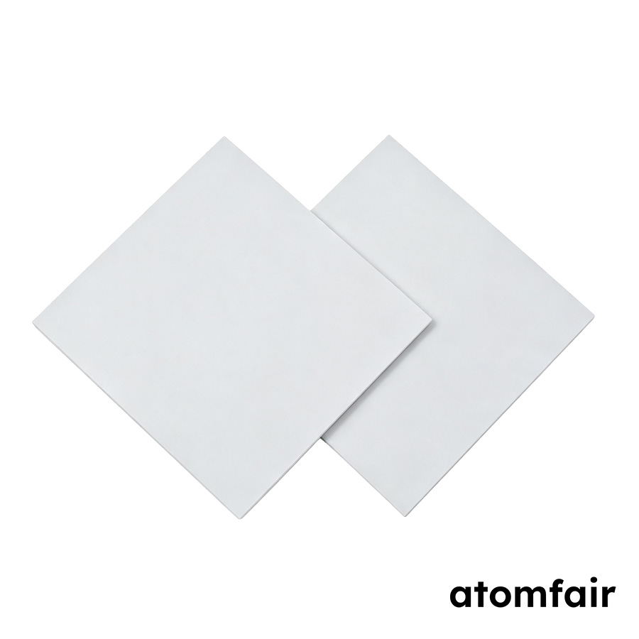
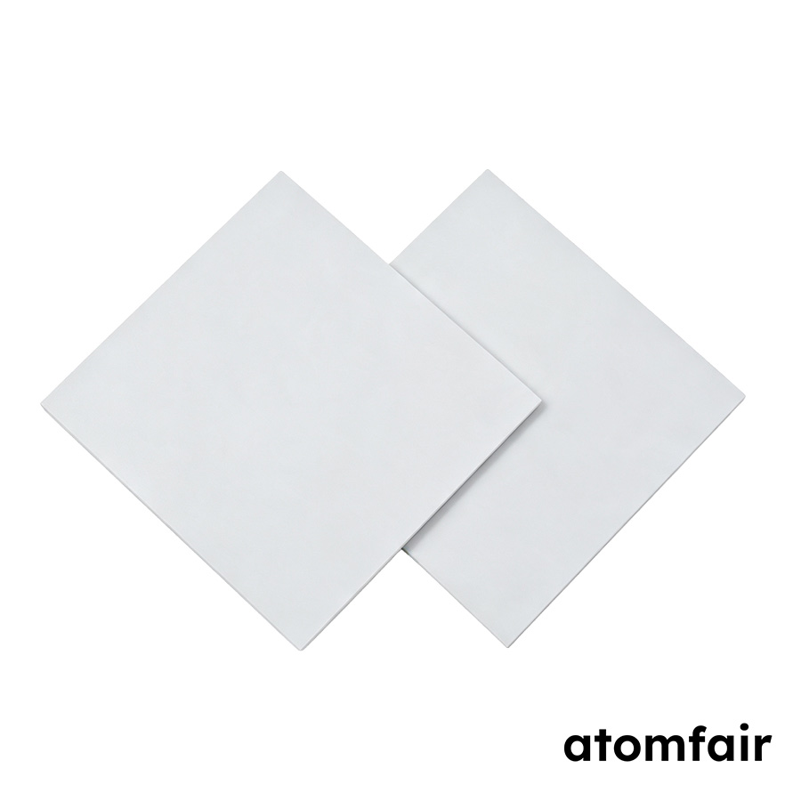
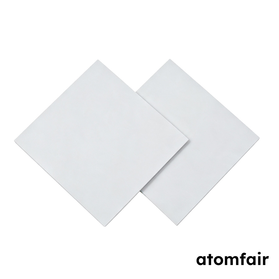
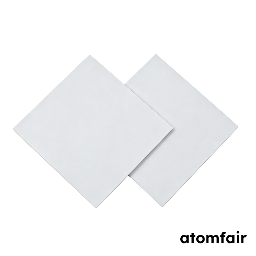
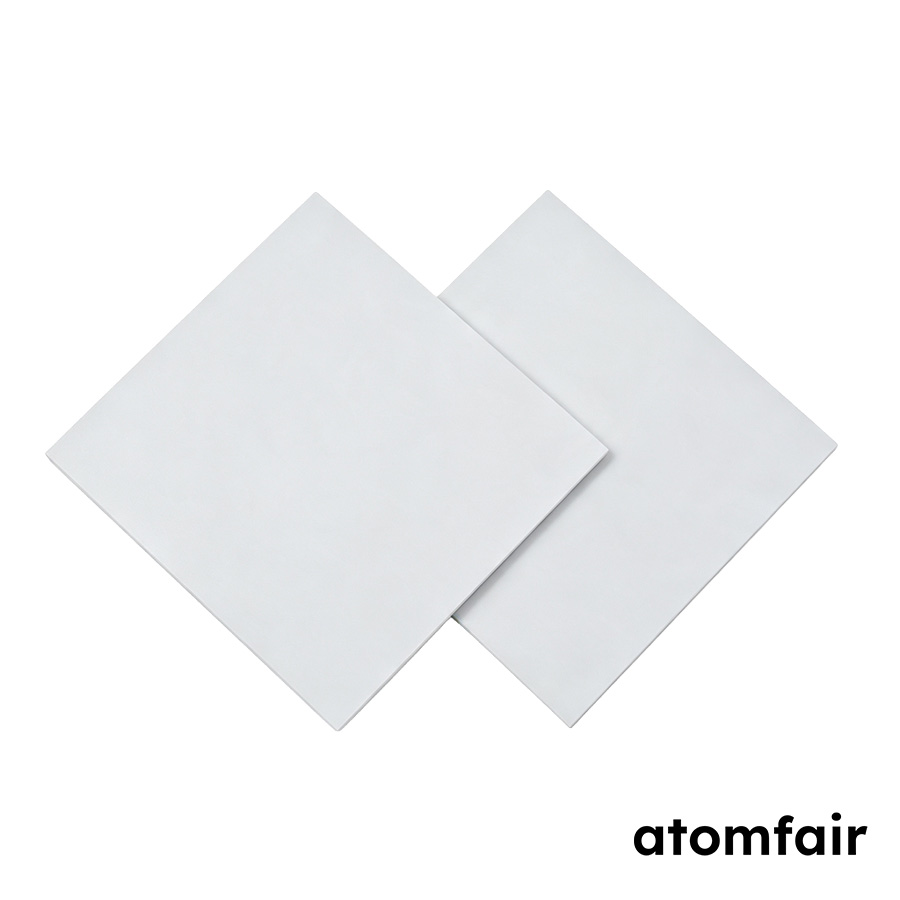
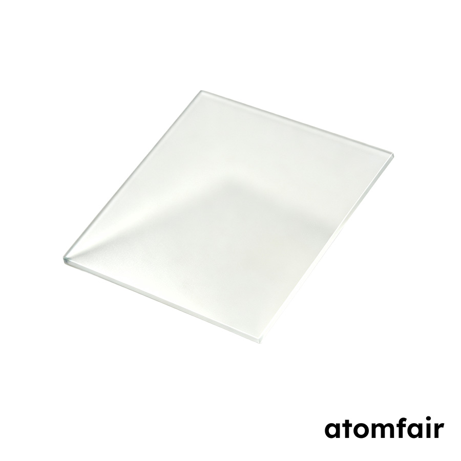
Yttrium Aluminum Garnet Single Crystal Substrate, SSP (10 pcs/box)
Product Type: YAG single crystal substrate
Research-grade laboratory product
|
|||||||||||||||||||||||||||||||||||||||||||||||||||
|
|||||||||||||||||||||||||||||||||||||||||||||||||||
|
LABORATORY PROCUREMENT SUPPORT
For material matching, specification review, model selection or configuration confirmation, contact our technical sales team.
E-MAIL: inquiry@atomfair.com
|
|||||||||||||||||||||||||||||||||||||||||||||||||||
|
Manufacturer: Atomfair LLC
Brand: ATOMFAIR®
|
This substrate requires careful material matching to the target thin-film or device workflow. All geometric and crystallographic parameters must be confirmed before use.
- Material Matching: Confirm that the substrate material and crystal family match the target thin-film or device workflow to ensure epitaxial compatibility and prevent performance degradation.
- Specification Review: Verify orientation, dimensions, thickness, polishing condition, offcut details, quantity, and any custom requirements for the selected specification option before ordering.
- Thermal and Lattice Compatibility: Evaluate the substrate's lattice constant and thermal expansion coefficient against the target thin-film material to minimize strain and avoid delamination during deposition.
What is the lattice constant of the YAG single crystal substrate and how does it affect epitaxial growth of garnet thin films?
The YAG single crystal substrate has a cubic crystal structure with a lattice constant of a = 12.01 Å. This lattice parameter is critical for lattice-matched epitaxial growth of garnet-based thin films such as YIG or rare-earth-doped garnets, as mismatch can induce strain or defects. The source specifies a crystal purity >99.999% and a cubic structure, supporting high-quality epitaxy.
Is the YAG substrate suitable for mid-infrared optical applications given its transmission range?
Yes, the YAG substrate transmits from 250 nm to 5000 nm, covering the visible, near-IR, and part of the mid-IR. The source notes no obvious absorption in the 2000-3000 nm range, making it suitable for applications like IR windows or optical components in that spectral region. Additionally, the dn/dt of 7.4×10⁻⁶/°C indicates minimal thermal lensing in high-power setups.
What is the thermal conductivity of the YAG substrate and why is it important for high-power laser or LED devices?
The YAG substrate has a thermal conductivity of 143 W/(m·K) at 20°C, which is relatively high for an oxide crystal. This facilitates efficient heat dissipation in high-power laser or LED devices, reducing thermal stress and enabling stable operation. The thermal expansion coefficient of 6.9×10⁻⁶/°C over 0-250°C also indicates moderate expansion behavior.
YAG single crystal substrate with SSP surface finish, available in 10×10×0.5 mm and 20×20×0.5 mm options, offering >99.999% purity, high thermal conductivity of 143 W/(m·K), and wide transmission range from 250 to 5000 nm for optical and thin-film applications.
Positive
- High purity and thermal stability: With >99.999% purity and a melting point of 1970°C, this substrate is suitable for high-temperature thin-film deposition processes without significant contamination risk.
- Broad optical transmission range: Transmits from 250 to 5000 nm with no obvious absorption in the 2000-3000 nm range, making it useful for infrared and visible optical applications.
Trade-offs
- Application-specific material matching required: The substrate material and crystal family must be confirmed to match the target thin-film or device workflow; improper matching can lead to lattice mismatch or thermal expansion incompatibility.
- Specification review needed for custom parameters: Orientation, dimensions, thickness, polishing condition, and offcut details must be verified before ordering; the listed options are only standard sizes and may not suit all applications.
Every advanced material, component, equipment, and instrument in our catalog is backed by rigorous testing. We maintain strict internal quality management frameworks and align with CE conformity metrics to deliver transparent, reproducible performance data via our public open-science repository.
To request raw batch performance data, submit formal vendor registration paperwork, or execute a fast-turnaround R&D manufacturing loop, contact us at inquiry@atomfair.com.
Item is dispatched under the Atomfair Shipping & Delivery Framework (Free worldwide shipping on orders over $59 USD excl. heavy equipment). Return is governed by the Atomfair Return & Refund Policy (7-day technical return window).