|
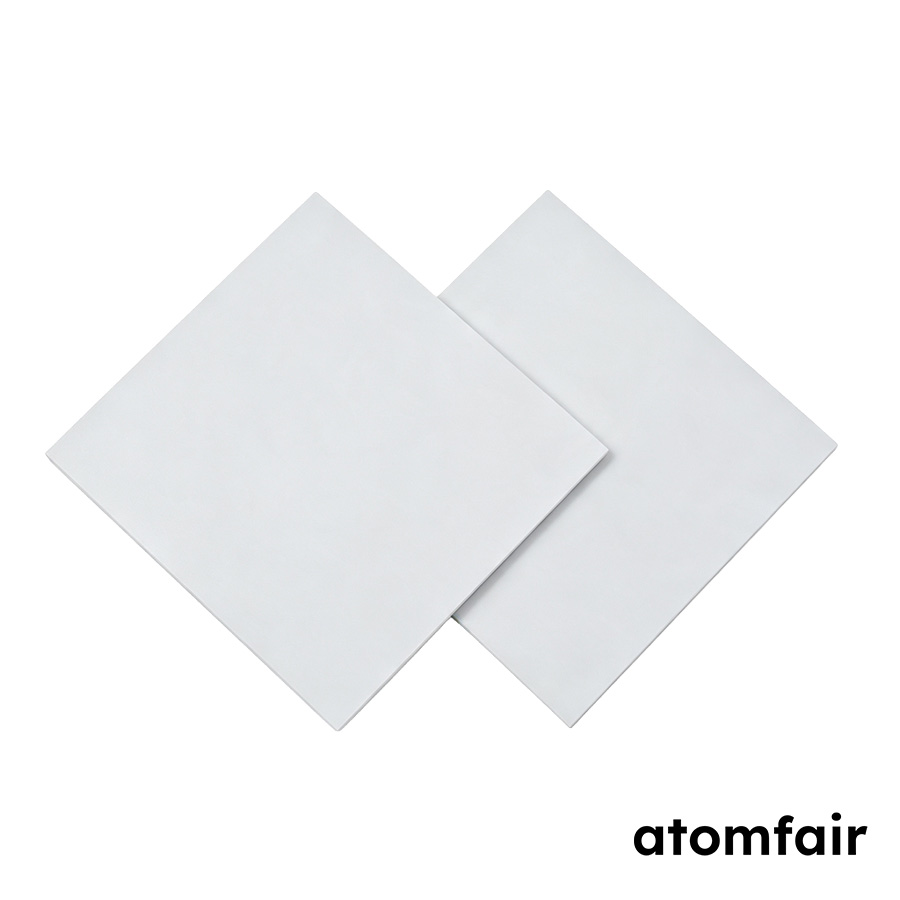
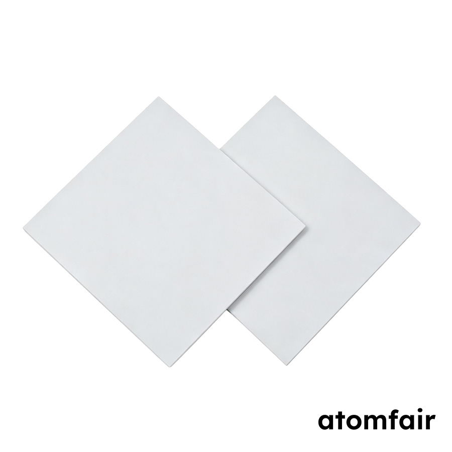
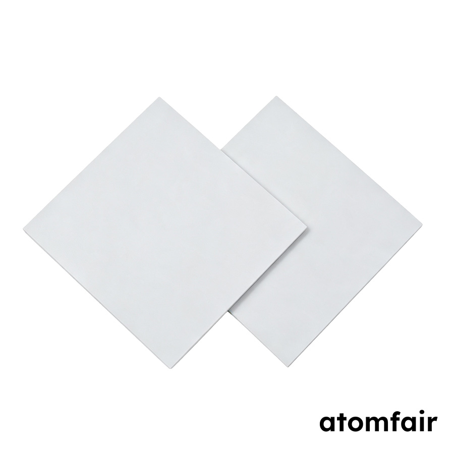
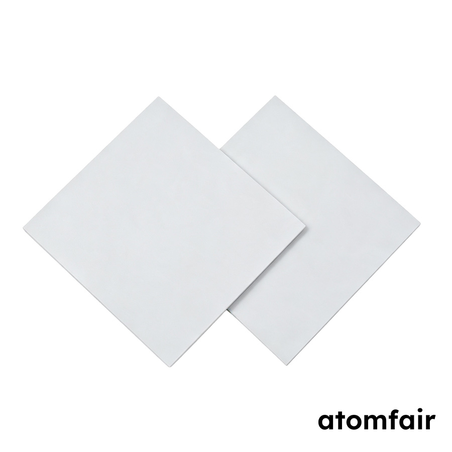
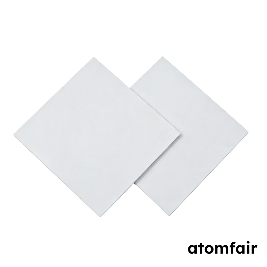
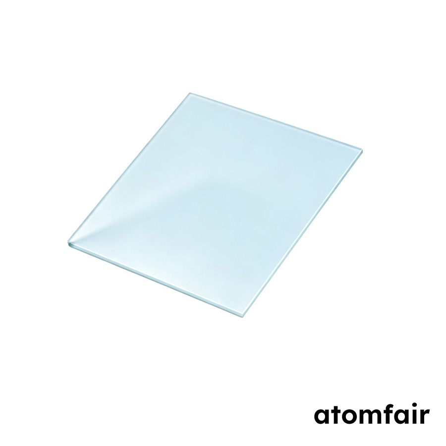
Strontium Titanate Single Crystal Substrate, 5 × 5 × 0.5 mm, DSP (10 pcs/box)
Product Type: SrTiO3 single crystal substrate
Research-grade laboratory product
|
|||||||||||||||||||||||||||||||||||||||||||
|
|||||||||||||||||||||||||||||||||||||||||||
|
LABORATORY PROCUREMENT SUPPORT
For model selection, accessory matching, platform compatibility or configuration confirmation, contact our technical sales team.
E-MAIL: inquiry@atomfair.com
|
|||||||||||||||||||||||||||||||||||||||||||
|
Manufacturer: Atomfair LLC
Brand: ATOMFAIR®
|
The substrate surface roughness is Ra < 5 Å and requires cleanroom-grade handling to avoid contamination or scratching. The material is water-insoluble but may exhibit slight brown discoloration depending on annealing history, indicating sensitivity to thermal processing conditions.
- Surface Integrity Constraint: Double-side polished surfaces with Ra < 5 Å demand particulate-free handling and storage to maintain optical and epitaxial quality.
- Thermal History Sensitivity: Annealing condition can alter substrate appearance, which may affect optical transmission consistency for thin-film deposition.
This procedure outlines substrate inspection, cleaning, and mounting steps prior to thin-film deposition. Proper handling prevents surface damage and ensures lattice-matched epitaxial growth.
Required Equipment: Cleanroom tweezers, Nitrogen blow gun
- Inspect Substrate Surface
Inspect the double-side polished substrate under an optical microscope for scratches, particles, or residues before any processing step. - Clean Substrate
Rinse the substrate sequentially in acetone, isopropanol, and deionized water using ultrasonic agitation for five minutes per solvent. - Dry Substrate
Dry the substrate with a stream of filtered nitrogen gas, holding it at a 45-degree angle to avoid liquid pooling. - Mount Substrate
Mount the cleaned substrate onto the deposition stage using a cleanroom-compatible adhesive or mechanical clamp, ensuring full thermal contact.
What is the surface roughness of the SrTiO3 substrate and how does it impact thin film quality?
The double-side polished (DSP) SrTiO3 substrate has a surface roughness of Ra < 5 Å, as specified in the technical data. This ultra-smooth finish minimizes scattering and defect nucleation during epitaxial growth, making it suitable for high-quality oxide thin films and high-temperature superconducting layers.
Which perovskite materials are lattice-matched to this SrTiO3 single crystal substrate?
The substrate has a cubic crystal structure with a lattice constant of a = 3.905 Å, providing lattice matching support for multiple perovskite materials commonly used in oxide thin film and superconductor research. The flame-method growth ensures twin-free crystallinity, critical for coherent epitaxy.
What are the handling and storage requirements for SrTiO3 substrates given their chemical and thermal properties?
SrTiO3 is chemically stable and insoluble in water, so no special humidity control is required for storage. However, its thermal expansion coefficient of 9.4 × 10⁻⁶ /°C and melting point of 2080°C mean that rapid temperature changes should be avoided to prevent thermal stress. The Mohs hardness of 6 indicates moderate scratch resistance; handle with clean tweezers or vacuum wand to maintain the Ra < 5 Å surface finish.
This SrTiO3 single crystal substrate provides a cubic perovskite structure with a lattice constant of 3.905 Å, enabling lattice-matched epitaxy for oxide thin films and high-temperature superconducting layers. The double-side polished surface (Ra < 5 Å) and high dielectric constant (300) with low loss tangent support advanced electronic and optical applications, though the small 5×5 mm area and annealing-dependent brown tint impose handling and application-specific constraints.
Positive
- Lattice-matched perovskite epitaxy: The cubic SrTiO3 structure with a = 3.905 Å provides direct lattice matching for many perovskite materials, enabling high-quality epitaxial growth of oxide thin films and superconducting layers.
- High dielectric constant with low loss: A dielectric constant of 300 combined with loss tangent values of ~5×10⁻⁴ at 300 K and ~3×10⁻⁴ at 77 K makes this substrate suitable for microwave and cryogenic electronic applications.
Trade-offs
- Annealing-dependent optical clarity: The substrate may exhibit a slight brown tint depending on annealing condition, which can reduce visible-light transmission and must be accounted for in optical window or spectroscopy applications.
- Small substrate area limits throughput: The 5×5 mm footprint restricts sample size and may require specialized handling or alignment fixtures, reducing experimental throughput compared to larger standard dimensions.
Every advanced material, component, equipment, and instrument in our catalog is backed by rigorous testing. We maintain strict internal quality management frameworks and align with CE conformity metrics to deliver transparent, reproducible performance data via our public open-science repository.
To request raw batch performance data, submit formal vendor registration paperwork, or execute a fast-turnaround R&D manufacturing loop, contact us at inquiry@atomfair.com.
Item is dispatched under the Atomfair Shipping & Delivery Framework (Free worldwide shipping on orders over $59 USD excl. heavy equipment). Return is governed by the Atomfair Return & Refund Policy (7-day technical return window).