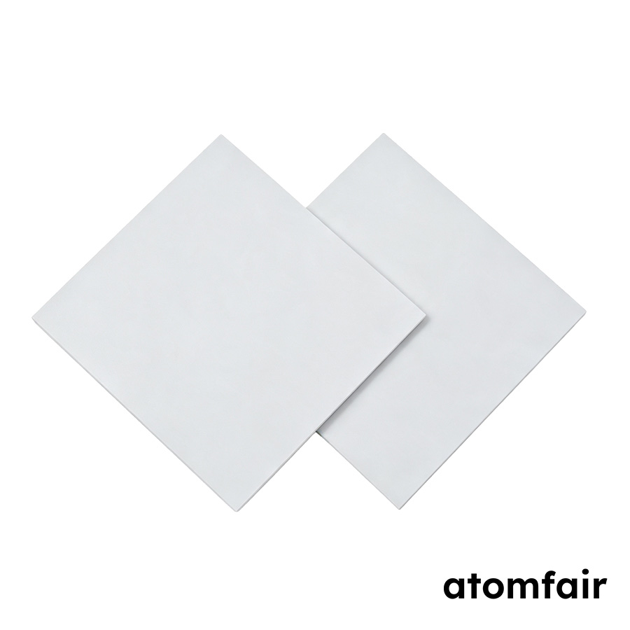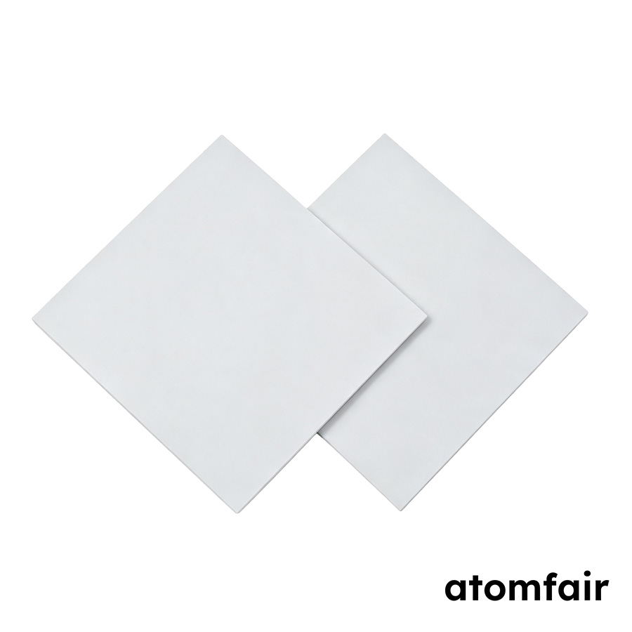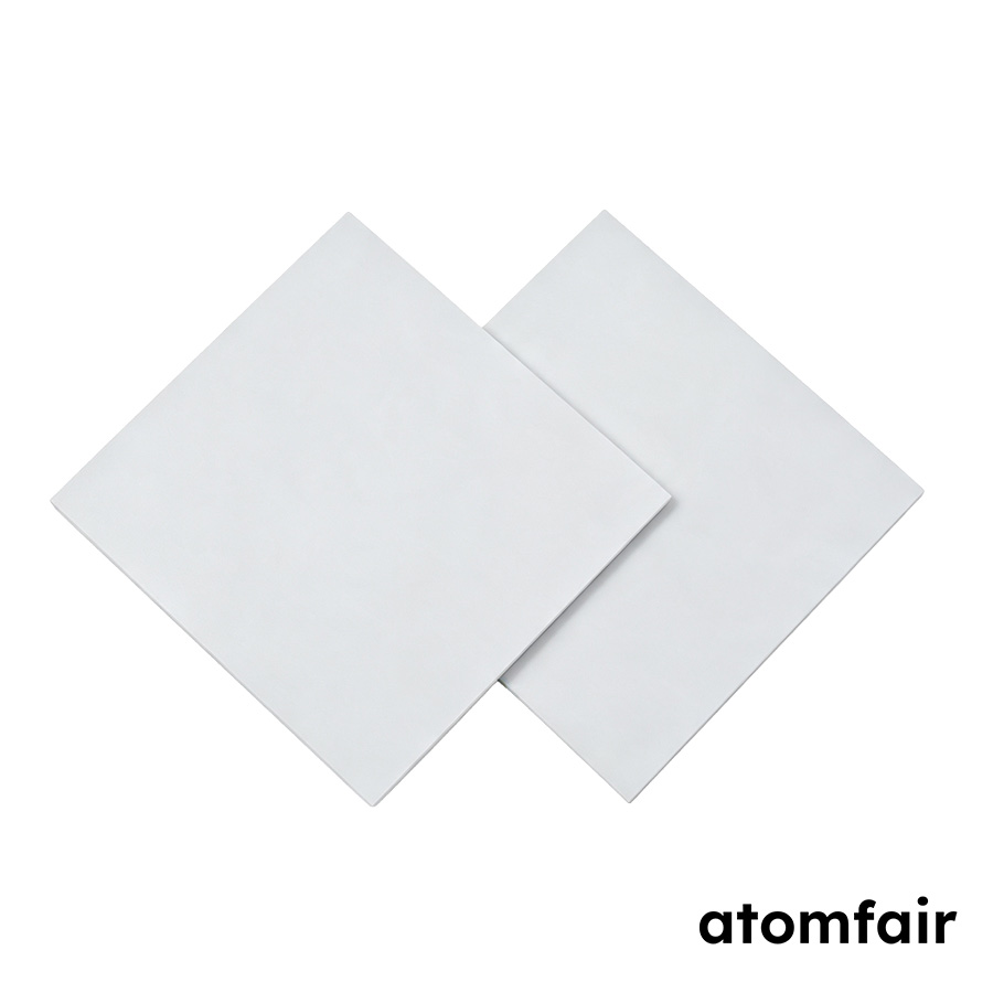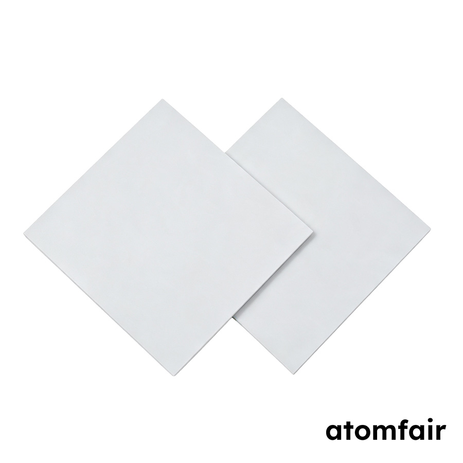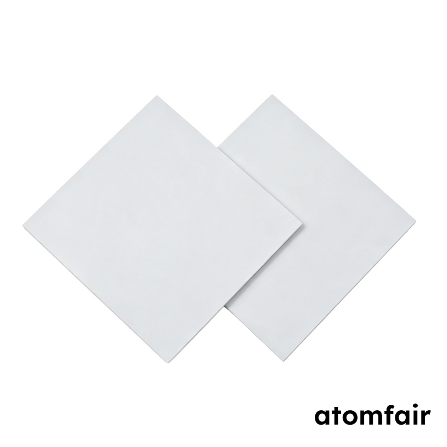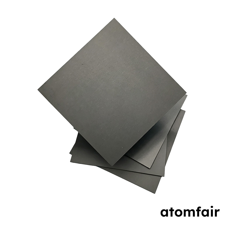
Silicon Nitride Ceramic Substrate, 114 mm x 114 mm x 0.25 mmProduct Type: Technical ceramic substrate
Research-grade laboratory product
|
|||||||||||||||||||||||||||||||||
|
|||||||||||||||||||||||||||||||||
|
LABORATORY PROCUREMENT SUPPORT
For model selection, accessory matching, platform compatibility or configuration confirmation, contact our technical sales team.
E-MAIL: inquiry@atomfair.com
|
|||||||||||||||||||||||||||||||||
|
Supplier: Atomfair
Brand: ATOMFAIR®
|
This substrate exhibits high flexural strength and fracture toughness but is susceptible to chipping or cracking under localized impact or improper clamping. Thermal shock resistance is limited by the material's thermal conductivity and coefficient of thermal expansion, requiring controlled heating and cooling rates.
- Thermal Management: Limit temperature ramp rates to avoid thermal shock when cycling between -55 °C and 850 °C.
- Mechanical Handling: Use padded or vacuum handling tools to prevent edge chipping or surface damage during placement.
- Surface Integrity: Avoid abrasive contact with the substrate surface to maintain dielectric breakdown strength above 15 kV/mm.
This procedure describes safe handling and preparation of a silicon nitride ceramic substrate for laboratory use. Proper technique minimizes mechanical damage and ensures electrical insulation performance.
Required Equipment: Vacuum pickup tool with silicone tip, Cleanroom-grade lint-free wipes, Isopropyl alcohol (IPA) for cleaning
- Inspect substrate
Visually inspect the substrate for cracks, chips, or surface contamination before handling. - Clean surface
Wipe the substrate gently with a lint-free wipe moistened with isopropyl alcohol to remove particulate residues. - Position substrate
Use a vacuum pickup tool to place the substrate onto a clean, flat, non-abrasive work surface. - Secure for processing
Clamp the substrate evenly along its edges using soft-jawed fixtures to avoid stress concentration. - Apply thermal load
Heat or cool the substrate at a controlled rate not exceeding 10 °C per minute to prevent thermal shock.
Can this silicon nitride ceramic substrate withstand high mechanical stress and high heat flux simultaneously?
Yes. The substrate is rated for high mechanical stress with stable shape retention, featuring flexural strength above 600 MPa, Young's modulus above 310 GPa, and fracture toughness of 6.5 MPa·√m. It also provides thermal conductivity above 60 W/(m·K), supporting demanding ceramic substrate applications.
What configuration details and options must be confirmed before integrating this silicon nitride substrate into an application?
You must verify size tolerance, thickness requirement, material grade, surface finish, and package format for this 114 mm x 114 mm x 0.25 mm substrate. For integration-specific needs, also confirm any polishing, coating, metallization, or custom-shape requirements with the technical sales team.
What operating temperature and electrical insulation limits apply to this silicon nitride substrate?
The usable temperature range is -55 °C to 850 °C. The substrate provides a breakdown voltage greater than 15 kV/mm, ensuring high insulation in demanding ceramic substrate applications.
The AF-SIN-S114P025 silicon nitride ceramic substrate (114 mm x 114 mm x 0.25 mm) provides a flexural strength >600 MPa, fracture toughness of 6.5 MPa√m, and thermal conductivity >60 W/(m·K) for demanding structural and thermal management applications, though its thin profile requires careful handling to avoid edge chipping.
Positive
- High mechanical and thermal performance: Flexural strength >600 MPa and thermal conductivity >60 W/(m·K) enable reliable operation under thermal cycling and mechanical load in high-power electronics or substrate applications.
- Broad operating temperature range: Usable from -55 °C to 850 °C, allowing deployment in cryogenic to high-temperature laboratory or industrial environments without degradation of mechanical integrity.
Trade-offs
- Thin substrate handling fragility: At 0.25 mm thickness, the substrate is prone to fracture from localized stress or mishandling during integration, necessitating careful fixturing and edge protection during assembly.
- Customization requires configuration confirmation: Additional processing such as polishing, coating, or metallization must be verified with the supplier, adding lead time and requiring explicit specification of tolerances before procurement.
Every advanced material, component, equipment, and instrument in our catalog is backed by rigorous testing. We maintain strict internal quality management frameworks and align with CE conformity metrics to deliver transparent, reproducible performance data via our public open-science repository.
To request raw batch performance data, submit formal vendor registration paperwork, or execute a fast-turnaround R&D manufacturing loop, contact us at inquiry@atomfair.com.
Item is dispatched under the Atomfair Shipping & Delivery Framework (Free worldwide shipping on orders over $59 USD excl. heavy equipment). Return is governed by the Atomfair Return & Refund Policy (7-day technical return window).