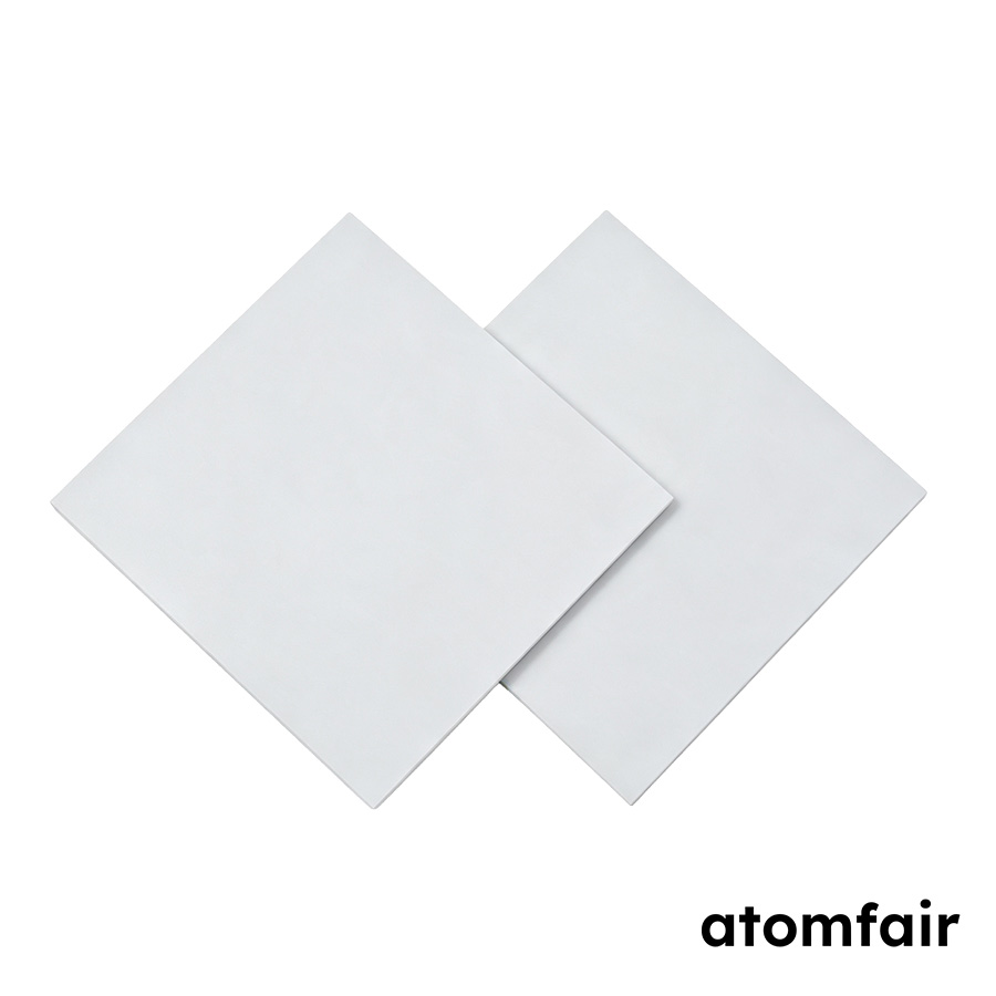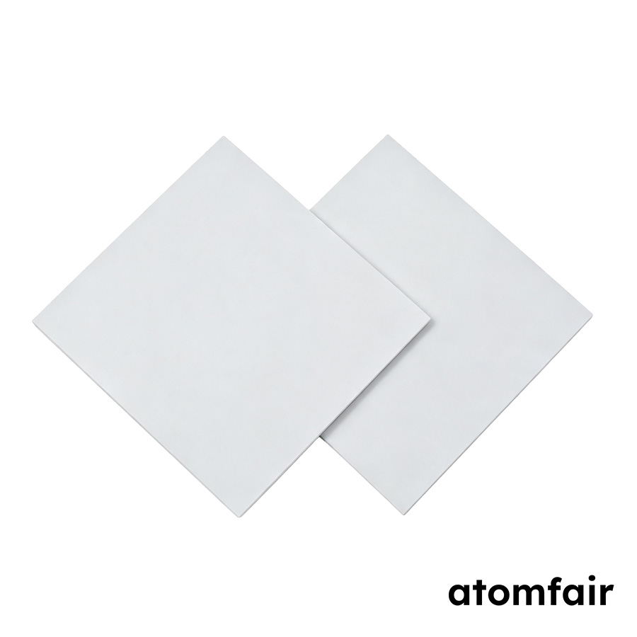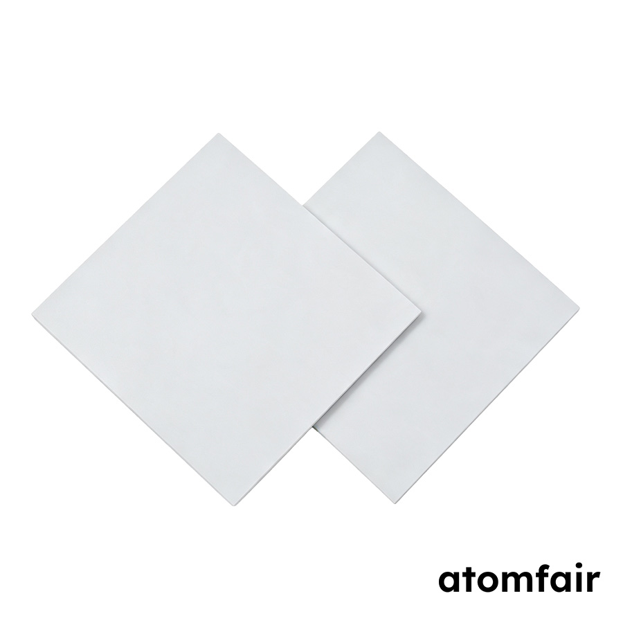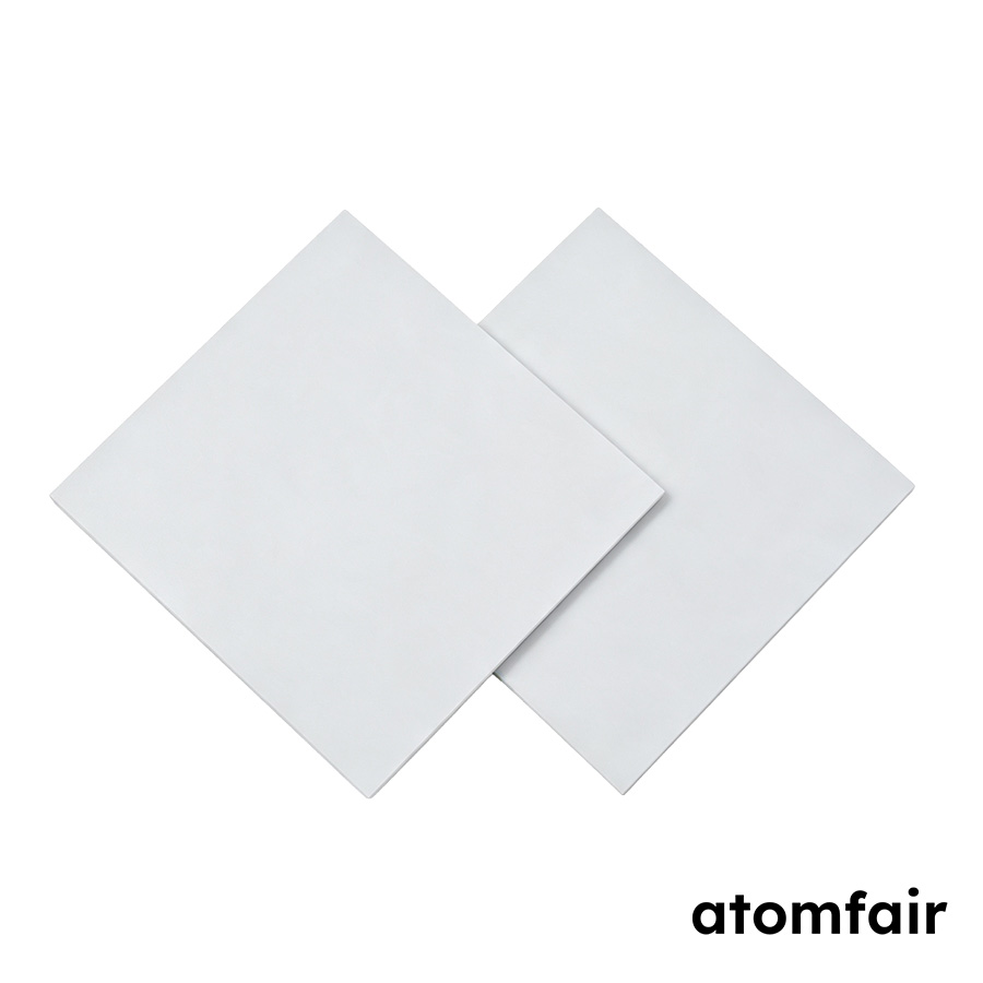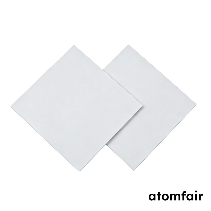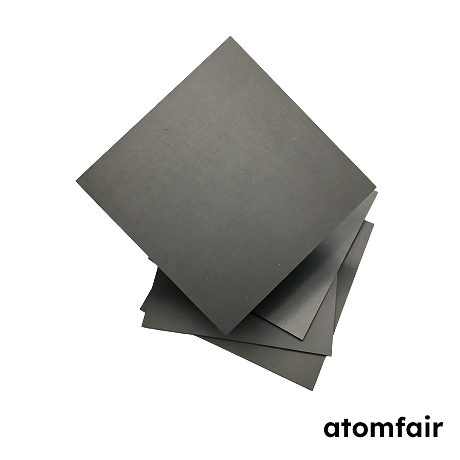
Silicon Nitride Ceramic Substrate, 100 mm x 100 mm x 0.635 mmProduct Type: Technical ceramic substrate
Research-grade laboratory product
|
|||||||||||||||||||||||||||||||||
|
|||||||||||||||||||||||||||||||||
|
LABORATORY PROCUREMENT SUPPORT
For model selection, accessory matching, platform compatibility or configuration confirmation, contact our technical sales team.
E-MAIL: inquiry@atomfair.com
|
|||||||||||||||||||||||||||||||||
|
Supplier: Atomfair
Brand: ATOMFAIR®
|
This substrate must be kept within its rated thermal and electrical operating limits to avoid mechanical or dielectric failure. Verify dimensional tolerances, surface finish, material grade, and packaging before installation.
- Thermal stability: Do not use the substrate at temperatures outside its rated use range.
- Electrical withstand: Do not apply electric field stress higher than the rated breakdown voltage.
- Mechanical loading: Apply mounting forces evenly to avoid concentrated loads that exceed the material's mechanical strength.
- Configuration verification: Confirm size tolerance, thickness, material grade, surface finish, and package format before installation.
What is the maximum operating temperature and thermal conductivity of the 100 mm x 100 mm x 0.635 mm silicon nitride ceramic substrate?
This silicon nitride substrate operates from -55 °C to 850 °C with a thermal conductivity above 60 W/(m·K). The high thermal conductivity combined with a flexural strength exceeding 600 MPa and fracture toughness of 6.5 MPa·√m makes it suitable for demanding thermal management and mechanical support applications in power electronics or high-temperature environments.
Does this 100 mm x 100 mm x 0.635 mm silicon nitride substrate require metallization or polishing for direct bonding to semiconductor devices?
The product is supplied as a bare technical ceramic substrate without pre-applied metallization, polishing, or coating. The product description explicitly states that polishing, coating, metallization, or custom-shape needs must be confirmed separately with the technical sales team. For direct bonding applications, you must specify these requirements during quotation to ensure compatibility with your assembly process.
What are the handling and storage requirements for this 0.635 mm thick silicon nitride ceramic substrate to prevent breakage?
Although the substrate offers high flexural strength above 600 MPa and fracture toughness of 6.5 MPa·√m, the 0.635 mm thickness requires careful handling to avoid edge chipping or cracking from point loads. The product description recommends confirming size tolerance, thickness requirement, material grade, surface finish, and package format before procurement. Standard clean-room handling with edge protection and cushioned storage is advised to maintain dimensional integrity.
The AF-SIN-S100P064 silicon nitride ceramic substrate (100 mm x 100 mm x 0.635 mm) provides flexural strength >600 MPa, fracture toughness of 6.5 MPa√m, and thermal conductivity >60 W/(m·K), making it suitable for high-stress, thermally demanding substrate applications. Its usable temperature range from -55 °C to 850 °C and high insulation with breakdown voltage >15 kV/mm define its operational envelope in lab and industrial settings.
Positive
- High mechanical and thermal resilience: Flexural strength above 600 MPa and fracture toughness of 6.5 MPa√m ensure resistance to mechanical stress and crack propagation; thermal conductivity above 60 W/(m·K) supports efficient heat dissipation in ceramic substrate applications.
- Broad operational temperature range: The substrate is rated for continuous use from -55 °C to 850 °C, enabling deployment in cryogenic to high-temperature environments without degradation of mechanical or insulation properties.
Trade-offs
- Requires confirmation of auxiliary processing: Polishing, coating, metallization, or custom shaping must be explicitly confirmed with the supplier before ordering, as these are not included by default and affect final part fit and performance.
- Size tolerance and surface finish verification needed: Buyers must verify size tolerance, thickness requirement, and surface finish parameters independently; the specified dimensions are nominal and may require tight-tolerance confirmation for precision assembly.
Every advanced material, component, equipment, and instrument in our catalog is backed by rigorous testing. We maintain strict internal quality management frameworks and align with CE conformity metrics to deliver transparent, reproducible performance data via our public open-science repository.
To request raw batch performance data, submit formal vendor registration paperwork, or execute a fast-turnaround R&D manufacturing loop, contact us at inquiry@atomfair.com.
Item is dispatched under the Atomfair Shipping & Delivery Framework (Free worldwide shipping on orders over $59 USD excl. heavy equipment). Return is governed by the Atomfair Return & Refund Policy (7-day technical return window).