|
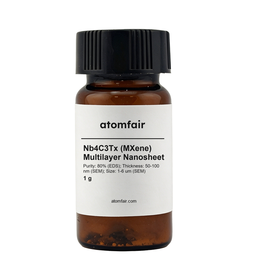
Nb4C3Tx (MXene) Multilayer Nanosheet, Package: 1 g
Product Type: MXene powder / nanosheet material
Research-grade laboratory product
|
|||||||||||||||||||
|
|||||||||||||||||||
|
LABORATORY PROCUREMENT SUPPORT
For material selection, specification confirmation and package-size quotation support, contact our technical sales team.
E-MAIL: inquiry@atomfair.com
|
|||||||||||||||||||
|
Supplier: Atomfair
Brand: ATOMFAIR®
|
Manufacturer: Atomfair LLC
Brand: ATOMFAIR®
What is the trade-off between sheet thickness and lateral size for Nb4C3Tx MXene multilayer nanosheets?
The Nb4C3Tx MXene multilayer nanosheets have a thickness of 50-100 nm (SEM) and lateral size of 1-6 µm (SEM). This relatively thick multilayer structure provides mechanical robustness but may limit accessible surface area compared to delaminated few-layer flakes, making it suitable for bulk applications rather than high-surface-area thin films.
How does the 80% purity (EDS) of Nb4C3Tx MXene constrain its use in electronic device fabrication?
The 80% purity measured by EDS indicates that the material contains residual etching byproducts or unexfoliated phases. For high-performance electronic devices requiring phase-pure MXene, additional purification steps may be necessary to remove these impurities.
What characterization infrastructure is required to verify the thickness and purity of Nb4C3Tx MXene multilayer nanosheets?
Thickness (50-100 nm) is verified using scanning electron microscopy (SEM), and purity (80%) is quantified using energy-dispersive X-ray spectroscopy (EDS). No additional specialized infrastructure beyond standard SEM/EDS equipment is required for routine quality control.
This Nb4C3Tx MXene multilayer nanosheet (1 g) provides a well-defined thickness range of 50–100 nm and lateral size of 1–6 μm, enabling controlled studies in energy storage or EMI shielding, though the 80% purity (EDS) and relatively thick multilayer form impose trade-offs in surface-area-dependent applications.
Positive
- Controlled nanosheet dimensions: Thickness of 50–100 nm and lateral size of 1–6 μm (SEM) provide reproducible morphology for comparative experiments in battery electrode or composite research.
- Niobium-based MXene chemistry: Nb4C3Tx offers distinct electronic and electrochemical properties relative to more common Ti3C2Tx, expanding the compositional space for fundamental MXene studies.
Trade-offs
- Moderate purity (80%): EDS-determined purity of 80% indicates ~20% non-MXene phases or residual byproducts, requiring users to account for potential interference in property measurements or performance metrics.
- Thick multilayer morphology: The 50–100 nm thickness corresponds to >10 stacked layers, reducing accessible surface area per mass compared to delaminated few-layer flakes, which may limit effectiveness in high-surface-area applications.
Every advanced material, component, equipment, and instrument in our catalog is backed by rigorous testing. We maintain strict internal quality management frameworks and align with CE conformity metrics to deliver transparent, reproducible performance data via our public open-science repository.
To request raw batch performance data, submit formal vendor registration paperwork, or execute a fast-turnaround R&D manufacturing loop, contact us at inquiry@atomfair.com.
Item is dispatched under the Atomfair Shipping & Delivery Framework (Free worldwide shipping on orders over $59 USD excl. heavy equipment). Return is governed by the Atomfair Return & Refund Policy (7-day technical return window).