|
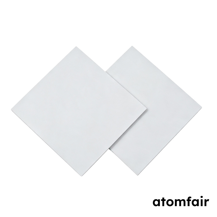
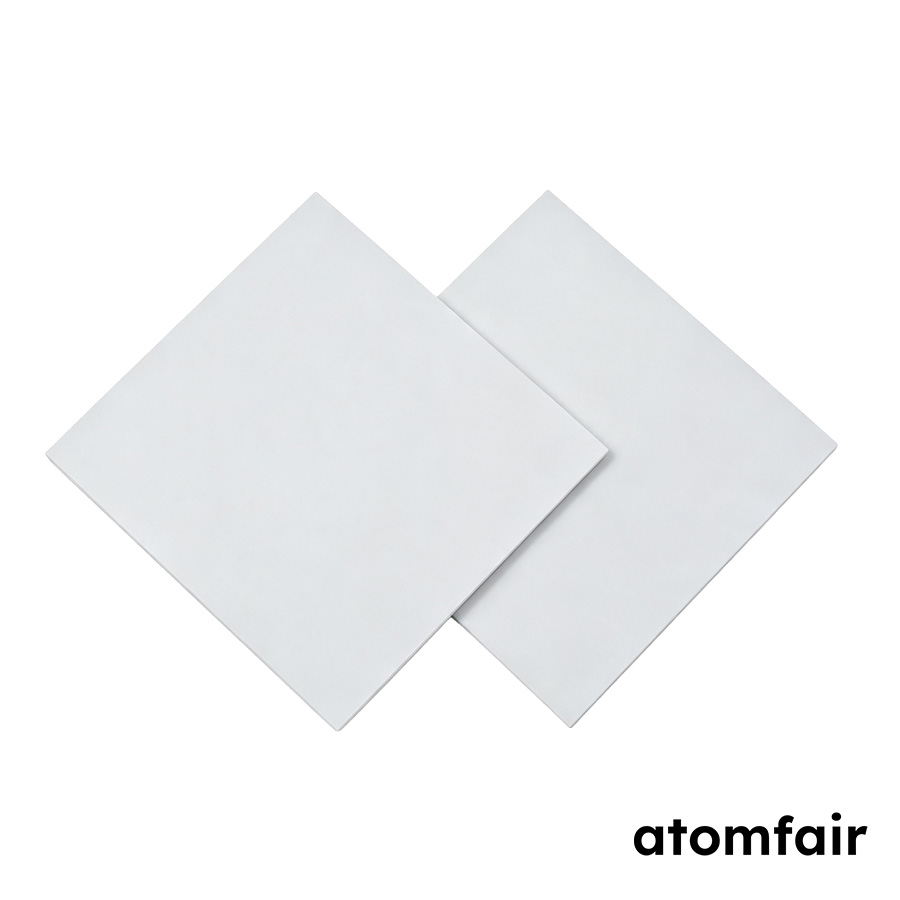
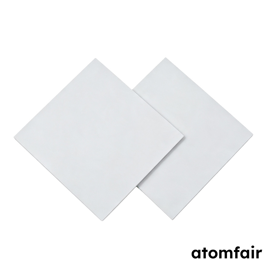
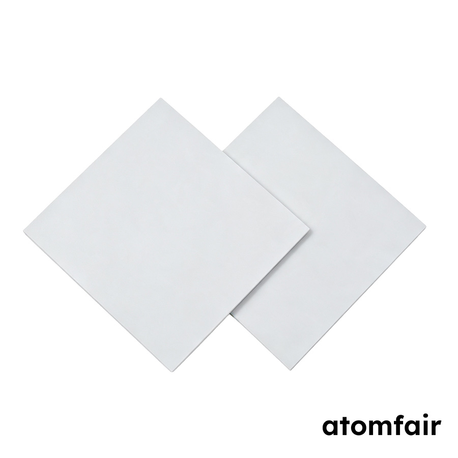
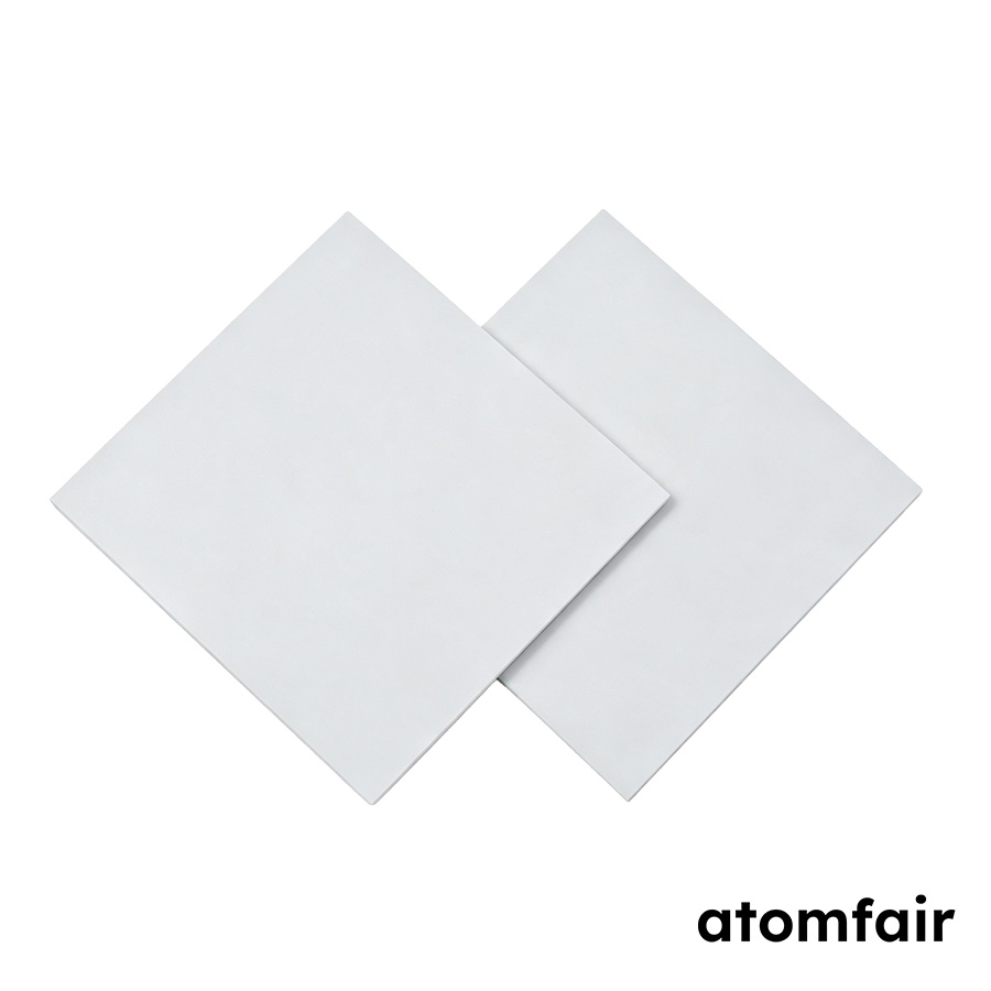
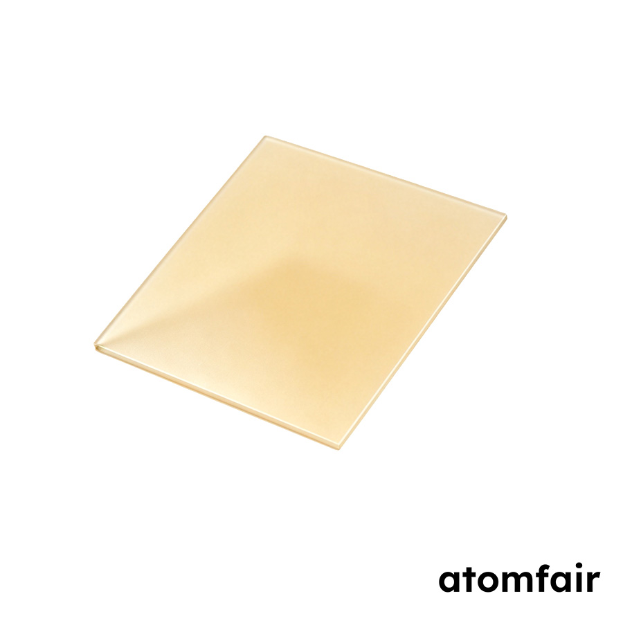
LSAT Single Crystal Substrate, (100), SSP (10 pcs/box)
Product Type: LSAT single crystal substrate
Research-grade laboratory product
|
|||||||||||||||||||||||||||||||||||||||||||||||||||
|
|||||||||||||||||||||||||||||||||||||||||||||||||||
|
LABORATORY PROCUREMENT SUPPORT
For material matching, specification review, model selection or configuration confirmation, contact our technical sales team.
E-MAIL: inquiry@atomfair.com
|
|||||||||||||||||||||||||||||||||||||||||||||||||||
|
Manufacturer: Atomfair LLC
Brand: ATOMFAIR®
|
This LSAT substrate requires careful material matching to the target thin-film workflow. Orientation tolerance and surface roughness must be verified for compatibility.
- Material Matching Requirement: Confirm that the substrate material and crystal family match the target thin-film or device workflow.
- Specification Review: Verify orientation, dimensions, thickness, polishing condition, offcut, and quantity against the selected option.
- Crystal Quality Constraint: The substrate must be twin-free with no visible domains for optimal thin-film growth.
What is the lattice constant of the LSAT (100) substrate and how does it influence material compatibility?
The lattice constant is a = 3.868 Å. This value is a key parameter for material matching to ensure crystallographic compatibility with the target thin-film or device, as emphasized in the product's material matching requirement. A close lattice match minimizes interfacial strain.
What are the available dimensions for the LSAT (100) substrate and how do they affect substrate selection?
The available specifications are 5 × 5 × 0.5 mm and 10 × 10 × 0.5 mm. Both share the same thickness of 0.5 mm and orientation (100). The choice of size depends on the required sample area for deposition or the constraints of the substrate holder.
This LSAT (100) single crystal substrate offers a twin-free, domain-free cubic structure with a lattice constant of 3.868Å and surface roughness below 5Å, making it suitable for epitaxial growth of oxide thin films. Availability in 0.5 mm thickness with two lateral dimensions (5×5 mm and 10×10 mm) accommodates common lab-scale deposition requirements.
Positive
- Ultra-smooth surface finish: Surface roughness Ra < 5Å enables high-quality epitaxial thin-film growth with minimal interfacial defects.
- High-temperature stability: Melting point of 1840°C and thermal expansion coefficient of 10 × 10⁻⁶/K support compatibility with high-temperature deposition processes.
Trade-offs
- Thin substrate fragility: 0.5 mm thickness requires careful handling during cutting, mounting, and transfer to avoid mechanical breakage.
- Mandatory material matching: Lattice constant (3.868Å) and chemical composition must be verified against target thin-film or device workflow to avoid lattice mismatch or chemical incompatibility.
Every advanced material, component, equipment, and instrument in our catalog is backed by rigorous testing. We maintain strict internal quality management frameworks and align with CE conformity metrics to deliver transparent, reproducible performance data via our public open-science repository.
To request raw batch performance data, submit formal vendor registration paperwork, or execute a fast-turnaround R&D manufacturing loop, contact us at inquiry@atomfair.com.
Item is dispatched under the Atomfair Shipping & Delivery Framework (Free worldwide shipping on orders over $59 USD excl. heavy equipment). Return is governed by the Atomfair Return & Refund Policy (7-day technical return window).