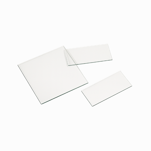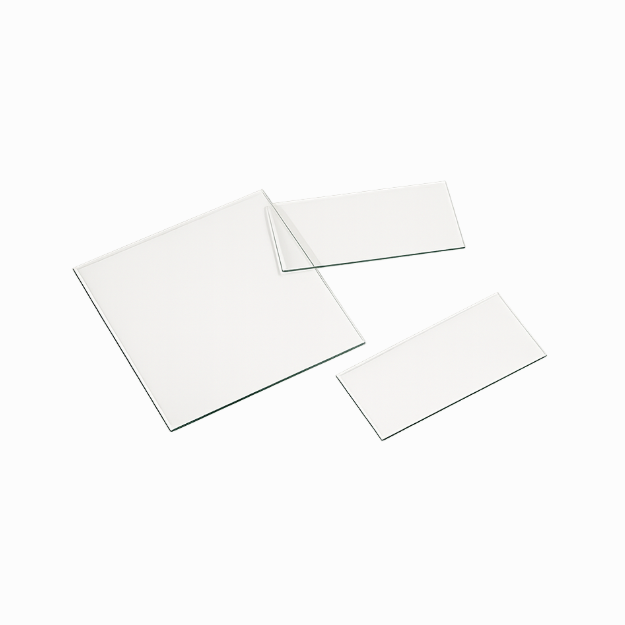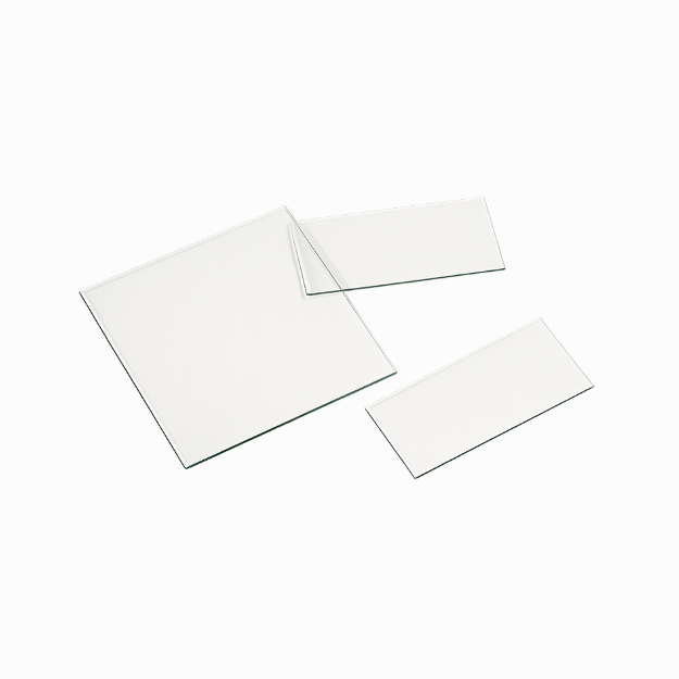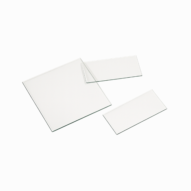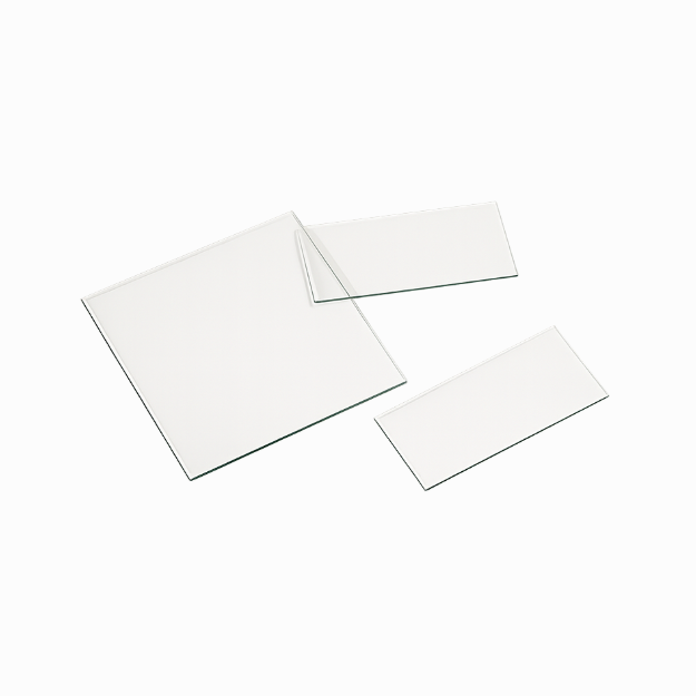
ITO Conductive Glass 7–10 Ω/sq 0.55mm 100 pcs ATOMFAIR®

Price range: $60.00 through $566.00

Institutional Procurement & Supply Compliance: As a verified US supplier, Atomfair accepts formal institutional Purchase Orders (POs), contract billing schedules, and custom procurement loops for university and national laboratories, and corporate R&D departments globally.

Magnetron-sputtered ITO conductive glass, 100 pcs, 0.55 mm thick with 7–10 Ω/sq sheet resistance for transparent electrodes. Order now.

ITO CONDUCTIVE GLASS 7-10 OHM 0.55MM 100 PCS MAGNETRON SPUTTERED

RESEARCH GRADE MATERIAL

Product Overview

This ITO Conductive Glass is manufactured by depositing an indium tin oxide thin film onto soda-lime or borosilicate base substrates via 7-10 Ohm magnetron sputtered coating technology. The product delivers excellent optical transmission with a wide bandgap, high visible-light transmittance, and stable electrical conductivity, making it a reliable optoelectronic device substrate for flat panel displays, solar cells, photoelectric window coatings, and various optoelectronic components. This listing is for 100 pieces at 0.55 mm thickness with 7–10 Ω/sq sheet resistance. Square resistance is customizable from 1 Ω to 10000 Ω, with substrate thickness ranging from 0.05 mm to 10 mm. The product supports free selection of base materials manufactured to specification. Full precision laser cutting custom processing services—including laser cutting, engraving, etching, hole drilling, edge grinding, and polishing—are available to meet exact dimensional and patterning requirements.

Technical Specifications

PARAMETER DETAILS
Material Type ITO (Indium Tin Oxide) Conductive Glass
Coating Process Magnetron Sputtering
Specification 100 Pieces
Thickness 0.55 mm
Square Resistance 7–10 Ω/sq
Custom Resistance Range 1 Ω–10000 Ω
Custom Thickness Range 0.05 mm–10 mm
Available Substrates Soda-Lime Float Glass / Ultra-White Glass / Borosilicate Glass / Quartz Glass / K9 Optical Glass / Sapphire Glass
Stock High-Borosilicate Substrates Asahi / SCHOTT / Corning (FTO/ITO Available)
Processing Services Laser Cutting / Engraving / Etching / Hole Drilling / Edge Grinding / Polishing / Ultrasonic Cleaning / Coating
Custom Shapes Square / Round / Hole / Slot / Irregular Workpieces
Custom Configurations Other substrate materials, dimensions, and processing specifications are available upon request. Please contact us via email for custom orders.

Key Features & Advantages

  • Extensive Substrate Material Selection: Available substrates include standard soda-lime float glass, ultra-white glass, borosilicate glass, quartz glass, K9 optical glass, and single-crystal sapphire. High-borosilicate substrates from Asahi, SCHOTT, and Corning are stocked regularly, with both FTO and ITO conductive coatings available.
  • Full-Range Resistance and Thickness Coverage: Square resistance from 1 Ω to 10000 Ω can be produced via magnetron sputtering. Substrate thickness spans from 0.05 mm ultra-thin sheets to 10 mm thick plates, matching the complete specification range required for diverse research and industrial applications.
  • Complete In-House Precision Processing: Integrated equipment for laser cutting, precision engraving, chemical etching, hole drilling, edge grinding, polishing, ultrasonic cleaning, and coating enables high-precision finished parts delivered from a single source, eliminating the need for multiple vendor coordination.
  • Flexible Custom Geometries and Markings: Supports square, round, hole-drilled, slotted, and irregular-shaped workpieces. Laser lettering, pattern etching, and precision cutting services allow device identification marking and custom electrode patterning directly on the coated substrate.

APPLICATION SCOPE: Transparent electrode substrate for flat panel display devices. Current collector for thin-film and perovskite solar cells. Photoelectric window coatings for sensors and detectors. Transparent conductive substrate for organic light-emitting diodes and optoelectronic components. Electrode platform for electrochemical biosensing and spectroelectrochemistry. EMI shielding windows for electronic instrumentation. The magnetron-sputtered ITO coating provides wide bandgap optical transparency combined with stable low-resistivity electrical performance across all application domains.
PACKAGING: This listing is for 100 pieces at 0.55 mm thickness with 7–10 Ω/sq sheet resistance. Each substrate is interleaved with cleanroom-grade lint-free separation film and packed in a rigid protective container to prevent mechanical damage and particulate contamination during transit. Custom resistance, thickness, substrate material, and processing specifications are manufactured to order. For bulk quantities or tailored configurations, please contact us via email.
IMPORTANT NOTICE: ITO conductive glass surfaces may accumulate dust, grease, and organic contaminants during production, packaging, and transport. Cleaning is mandatory before use. Handle substrates by the edges using cleanroom-compatible tweezers to avoid surface contamination of the ITO-coated side. For custom laser-cut or engraved pieces, verify dimensional tolerances and edge quality requirements at the time of order. Store unused substrates in a dry, dust-free environment to maintain surface cleanliness. For detailed cleaning protocols, consult the user guidelines provided with the shipment.
TAILORED SOLUTIONS FOR RESEARCH
Contact our engineering team for technical support or official quotations.
EMAIL: inquiry@atomfair.com
Manufacturer: Atomfair LLC
Brand: ATOMFAIR®

This ITO conductive glass substrate requires mandatory cleaning before use and careful handling to avoid surface contamination. Store unused substrates in a dry, dust-free environment to maintain surface cleanliness.

  • Surface Contamination Risk: ITO conductive glass surfaces may accumulate dust, grease, and organic contaminants during production, packaging, and transport.
  • Pre-Use Cleaning Requirement: Cleaning of the ITO-coated surface is mandatory before use to ensure optimal electrical and optical performance.
  • Handling Protocol: Handle substrates by the edges using cleanroom-compatible tweezers to avoid surface contamination of the ITO-coated side.
  • Storage Requirement: Store unused substrates in a dry, dust-free environment to maintain surface cleanliness and prevent degradation.
  • Custom Processing Verification: For custom laser-cut or engraved pieces, verify dimensional tolerances and edge quality requirements at the time of order.

Can this ITO conductive glass be used as a transparent electrode for perovskite solar cells?

Yes, the product is explicitly listed as a current collector for thin-film and perovskite solar cells. The magnetron-sputtered ITO coating provides wide bandgap optical transparency combined with stable low-resistivity electrical performance, making it suitable as a transparent electrode substrate.

What cleaning and handling procedures are recommended for ITO conductive glass substrates?

Cleaning is mandatory before use to remove dust, grease, and organic contaminants accumulated during production and transport. Handle substrates by the edges using cleanroom-compatible tweezers to avoid surface contamination. Store unused substrates in a dry, dust-free environment. Detailed cleaning protocols are provided with the shipment.

What custom processing services are available for patterning ITO-coated glass substrates?

The manufacturer offers in-house precision processing including laser cutting, engraving, chemical etching, hole drilling, edge grinding, polishing, ultrasonic cleaning, and coating. These services enable custom geometries such as squares, rounds, holes, slots, and irregular shapes, as well as laser lettering and pattern etching directly on the coated substrate.

This ITO conductive glass substrate (7–10 Ω/sq, 0.55 mm thickness) is magnetron-sputtered on soda-lime or borosilicate glass, offering high visible-light transmittance and stable electrical conductivity. Available in four sizes (10×10 to 100×100 mm) with full customization of resistance (1–10000 Ω), thickness (0.05–10 mm), substrate material, and precision laser processing, it serves as a versatile transparent electrode for optoelectronic devices, solar cells, and electrochemical sensors.

Positive

  • Extensive substrate material selection: Supports soda-lime, ultra-white, borosilicate, quartz, K9 optical, and sapphire glass substrates, with stocked high-borosilicate options from Asahi, SCHOTT, and Corning, enabling application-specific optical and thermal matching.
  • Full-range resistance and thickness customization: Square resistance tunable from 1 Ω to 10000 Ω and substrate thickness from 0.05 mm to 10 mm via magnetron sputtering, covering the complete specification range for diverse research and industrial requirements.

Trade-offs

  • Mandatory pre-use cleaning required: ITO surfaces accumulate dust, grease, and organic contaminants during production and transport; cleaning is mandatory before use to ensure reliable electrical and optical performance.
  • Strict handling and storage protocols: Substrates must be handled by edges with cleanroom tweezers to avoid surface contamination, and stored in a dry, dust-free environment to maintain cleanliness and functionality.

Every advanced material, component, equipment, and instrument in our catalog is backed by rigorous testing. We maintain strict internal quality management frameworks and align with CE conformity metrics to deliver transparent, reproducible performance data via our public open-science repository.

To request raw batch performance data, submit formal vendor registration paperwork, or execute a fast-turnaround R&D manufacturing loop, contact us at inquiry@atomfair.com.

Item is dispatched under the Atomfair Shipping & Delivery Framework (Free worldwide shipping on orders over $59 USD excl. heavy equipment). Return is governed by the Atomfair Return & Refund Policy (7-day technical return window).
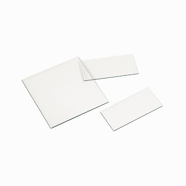
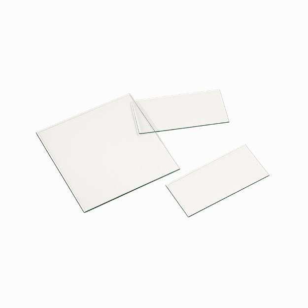
size

10×10×0.55mm, 20×20×0.55mm, 50×50×0.55mm, 100×100×0.55mm