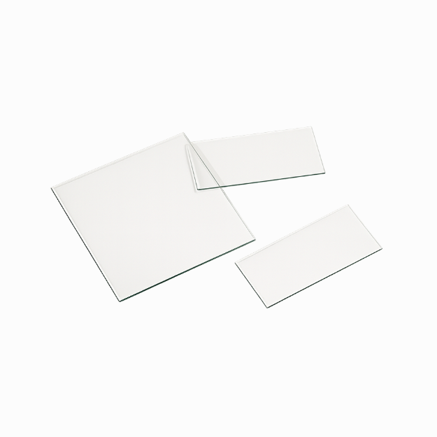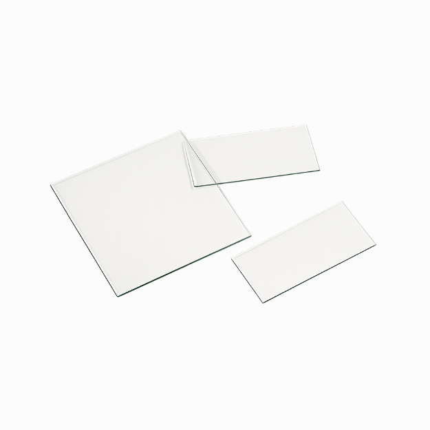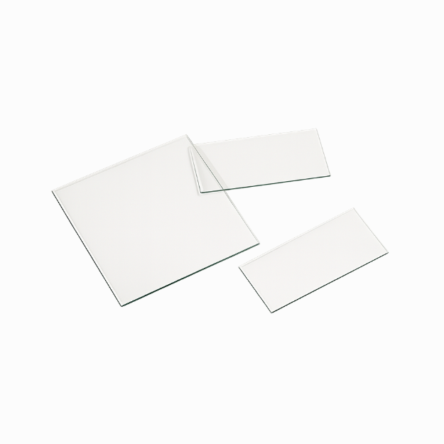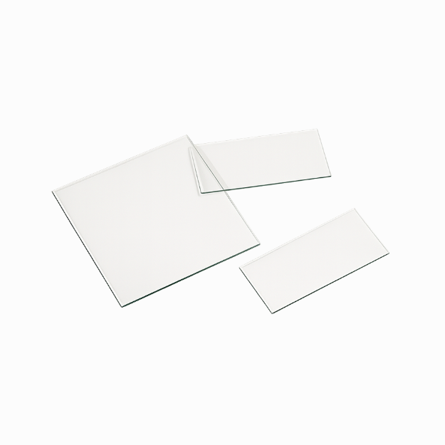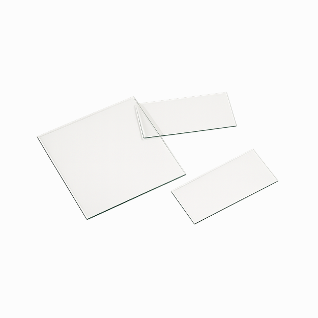
FTO Conductive Glass 7Ω/sq 350nm 2.2mm 100 pcs ATOMFAIR®

Price range: $65.00 through $638.00

Institutional Procurement & Supply Compliance: As a verified US supplier, Atomfair accepts formal institutional Purchase Orders (POs), contract billing schedules, and custom procurement loops for university and national laboratories, and corporate R&D departments globally.

Research grade FTO conductive glass, 7 Ω/sq with 350 nm SnO2:F coating on 2.2 mm glass; 80% transmittance, 600°C stability. Order now.

FTO CONDUCTIVE GLASS 7 OHM 2.2MM SNO₂:F 600°C 100 PCS

RESEARCH GRADE MATERIAL

Product Overview

This FTO Conductive Glass features a fluorine-doped tin oxide (SnO₂:F) transparent conductive coating with a 7 Ohm 350nm SnO₂:F coating deposited on a 2.2 mm glass substrate. SnO₂ is a wide-bandgap oxide semiconductor (3.7–4.0 eV) with a tetragonal rutile crystal structure; fluorine doping imparts low resistivity, excellent visible-light transparency exceeding 80%, strong UV absorption, and superior chemical stability with outstanding room-temperature acid corrosion resistance. The product withstands operating temperatures up to 600°C, making it the preferred transparent electrode for dye-sensitized solar cell substrate research where ITO’s thermal limitations preclude its use. This listing is for 100 pieces. Each substrate is individually film-laminated with the blue film side indicating the conductive surface, preventing coating scratches during handling and storage. Full CNC precision processing services are available for custom geometries.

Technical Specifications

PARAMETER DETAILS
Material Type FTO (Fluorine-Doped Tin Oxide, SnO₂:F) Conductive Glass
Conductive Surface Identification Blue Film-Laminated Side
Specification 100 Pieces
Square Resistance 7 Ω/sq
Coating Thickness 350 nm
Visible Light Transmittance 80%
Maximum Operating Temperature 600°C
Substrate Thickness 2.2 mm (Customizable)
Individual Packaging Single-Sheet Film Lamination
Custom Shapes Square / Round / Triangle / Trapezoid / Irregular Custom
Surface Flatness (Pre-Sinter) 1.225 μm / 9.287 μm
Surface Flatness (Post-Sinter) 3.375 μm / 11.225 μm
CNC Processing Services Cutting / Etching / Straight Edge / Round Edge / Corner Point / Scribing / Slotting / Hole Drilling / Laser Etching
Cutting Precision ≤0.05 mm Tolerance
Edge Treatment Options Right Angle / Safety Angle / Round Corner / Cut Corner / Beveled Edge
Processing Equipment CNC Cutter / Precision Engraver / Laser Machine / Edge Grinder
Custom Configurations Other substrate thicknesses, dimensions, and processing specifications are available upon request. Please contact us via email for custom orders.

Key Features & Advantages

  • 600°C High-Temperature Capability: Unlike ITO conductive glass which degrades above 300°C, the SnO₂:F coating remains stable up to 600°C, enabling high-temperature sintering of mesoporous TiO₂ layers in dye-sensitized solar cell fabrication and maintaining conductivity during thermal catalytic experiments.
  • Superior Chemical Stability: The fluorine-doped tin oxide coating exhibits outstanding room-temperature resistance to acid corrosion, making it the substrate of choice for photoelectrochemical experiments involving acidic electrolytes that would etch ITO coatings.
  • Individual Sheet Protective Lamination: Each substrate is individually film-laminated with the blue protective film clearly marking the conductive surface side, preventing coating scratches during storage, handling, and custom CNC processing while eliminating ambiguity in conductive surface identification.
  • High-Precision CNC Custom Processing: In-house CNC cutters, precision engravers, laser machines, and edge grinders deliver cutting tolerances of 0.05 mm or better, with multiple edge treatment options including right angle, safety angle, round corner, cut corner, and beveled edge for application-specific geometric requirements.

APPLICATION SCOPE: Transparent conductive substrate for dye-sensitized solar cells requiring high-temperature TiO₂ sintering. Working electrode for photocatalytic water splitting and organic pollutant degradation experiments. Transparent electrode for perovskite solar cells processed at elevated temperatures. Conductive substrate for electrochromic glass and smart window research. Transparent electrode for liquid crystal display prototypes and thin-film optoelectronic device fabrication. The 600°C thermal stability and acid-resistant SnO₂:F coating make FTO the standard substrate for any experimental workflow involving thermal processing or acidic electrolyte exposure where ITO coatings fail.
PACKAGING: This listing is for 100 pieces at 2.2 mm substrate thickness with 7 Ω/sq sheet resistance and 350 nm SnO₂:F coating. Each substrate is individually film-laminated (blue film side = conductive surface) and packed in a rigid protective container. Custom substrate thickness, dimensions, shapes, and CNC processing specifications are manufactured to order. For bulk quantities or tailored configurations, please contact us via email.
IMPORTANT NOTICE: Handle FTO substrates by the four edges only; never touch the conductive coated surface directly. The blue film-laminated side identifies the conductive surface—verify orientation before use. For long-term storage, maintain ambient humidity below 65% in a dry, shaded location away from direct sunlight to prevent degradation of sheet resistance and optical transmittance. Handle gently and avoid impact with hard tooling or equipment surfaces. When specifying custom CNC processing, provide detailed dimensional drawings with tolerance requirements. Post-sintering surface flatness values (3.375 μm / 11.225 μm) should be considered in device architectures requiring precise layer thickness control. For detailed cleaning and usage protocols, consult the user guidelines provided with the shipment.
TAILORED SOLUTIONS FOR RESEARCH
Contact our engineering team for technical support or official quotations.
EMAIL: inquiry@atomfair.com
Manufacturer: Atomfair LLC
Brand: ATOMFAIR®

Store FTO substrates in a dry environment with humidity below 65% and away from direct sunlight to prevent degradation of sheet resistance and optical transmittance. Handle substrates by the four edges only and avoid contact with the conductive coated surface to prevent scratches and contamination.

  • Humidity Control: Maintain ambient humidity below 65% during storage to prevent degradation of electrical and optical properties.
  • Light Exposure: Store in a shaded location away from direct sunlight to avoid UV-induced degradation of the SnO₂:F coating.
  • Handling Method: Handle FTO substrates by the four edges only and never touch the conductive coated surface.
  • Conductive Surface Identification: The blue film-laminated side indicates the conductive surface; verify orientation before use.
  • Post-Sintering Flatness: Consider post-sintering surface flatness values (3.375 μm / 11.225 μm) in device architectures requiring precise layer thickness control.

Follow these steps to properly handle and store FTO conductive glass substrates to maintain their electrical and optical properties. Adherence to these guidelines prevents damage from contamination, humidity, and light exposure.

Required Equipment:

  1. Inspect the Substrate
    Inspect the blue film-laminated side of each substrate to confirm the conductive surface orientation before use.
  2. Handle by Edges
    Handle the substrate by the four edges only to avoid touching the conductive coated surface.
  3. Store in Controlled Environment
    Store the substrates in a dry, shaded location with ambient humidity below 65% and away from direct sunlight.

Why choose FTO over ITO for high-temperature applications?

FTO conductive glass is preferred over ITO for applications requiring high-temperature processing because the SnO₂:F coating remains stable up to 600°C, whereas ITO degrades above 300°C. This makes FTO essential for dye-sensitized solar cell fabrication involving sintering of mesoporous TiO₂ layers at elevated temperatures.

How do I identify the conductive side of the FTO substrate?

The blue film-laminated side indicates the conductive surface. Each substrate is individually film-laminated with the blue film side marking the conductive side, preventing coating scratches and eliminating ambiguity in orientation during handling and processing.

What are the recommended storage and handling conditions for FTO conductive glass?

Store FTO substrates in a dry, shaded location with ambient humidity below 65% and away from direct sunlight to prevent degradation of sheet resistance and optical transmittance. Handle substrates by the four edges only to avoid touching the conductive coated surface.

This FTO conductive glass (7 Ω/sq, 350 nm SnO₂:F on 2.2 mm substrate) is engineered for high-temperature and acidic-electrolyte applications where ITO fails. Its 600°C thermal stability enables direct sintering of mesoporous TiO₂ layers for dye-sensitized solar cells, while the fluorine-doped coating provides superior acid resistance for photoelectrochemical experiments. The 100-piece lot includes individual protective lamination and supports custom CNC processing with ≤0.05 mm tolerance.

Positive

  • 600°C thermal stability: The SnO₂:F coating remains stable up to 600°C, enabling high-temperature sintering of mesoporous TiO₂ layers in dye-sensitized solar cell fabrication, unlike ITO which degrades above 300°C.
  • Acid-resistant conductive coating: The fluorine-doped tin oxide exhibits outstanding room-temperature resistance to acid corrosion, making it the preferred substrate for photoelectrochemical experiments involving acidic electrolytes that would etch ITO coatings.

Trade-offs

  • Strict handling requirements: Substrates must be handled only by the four edges; direct contact with the conductive coated surface is prohibited. The blue film-laminated side identifies the conductive surface and must be verified before use to avoid orientation errors.
  • Controlled storage conditions needed: Long-term storage requires ambient humidity below 65% in a dry, shaded location away from direct sunlight to prevent degradation of sheet resistance and optical transmittance. Post-sintering surface flatness (3.375 μm / 11.225 μm) must be considered in device architectures requiring precise layer thickness control.

Every advanced material, component, equipment, and instrument in our catalog is backed by rigorous testing. We maintain strict internal quality management frameworks and align with CE conformity metrics to deliver transparent, reproducible performance data via our public open-science repository.

To request raw batch performance data, submit formal vendor registration paperwork, or execute a fast-turnaround R&D manufacturing loop, contact us at inquiry@atomfair.com.

Item is dispatched under the Atomfair Shipping & Delivery Framework (Free worldwide shipping on orders over $59 USD excl. heavy equipment). Return is governed by the Atomfair Return & Refund Policy (7-day technical return window).
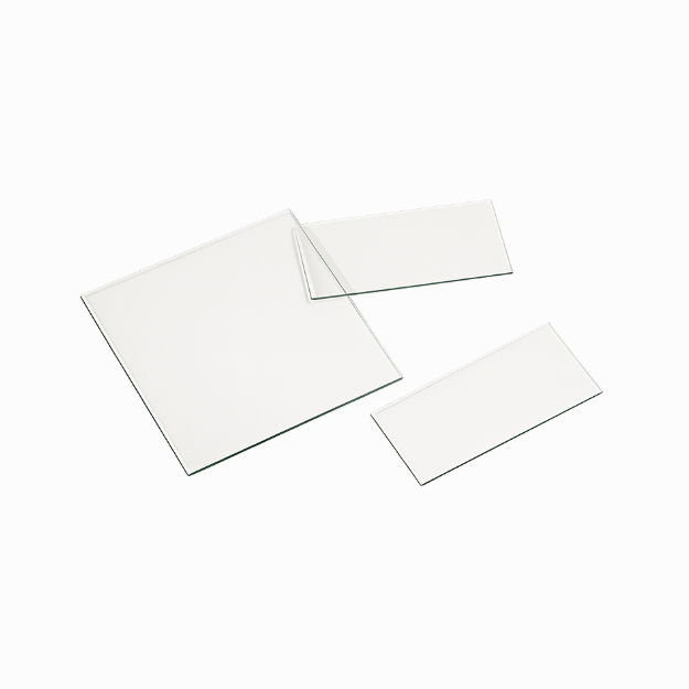
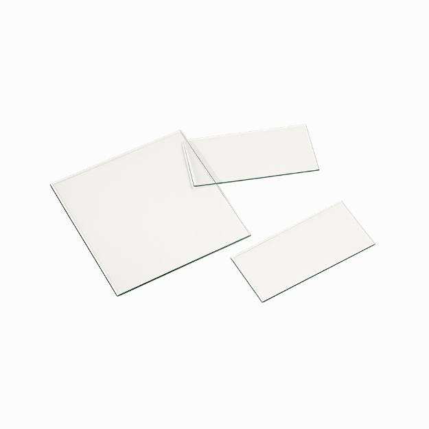
size

10×10×2.2mm, 20×20×2.2mm, 50×50×2.2mm, 100×100×2.2mm