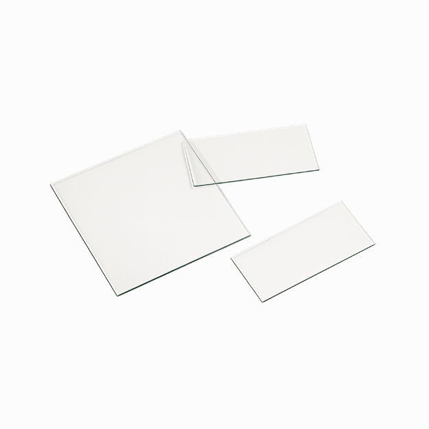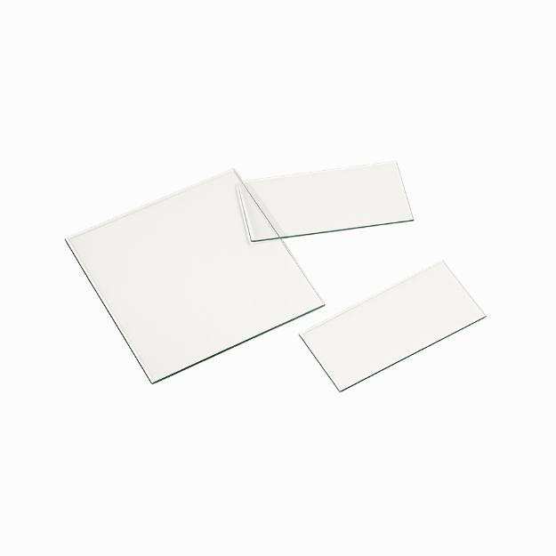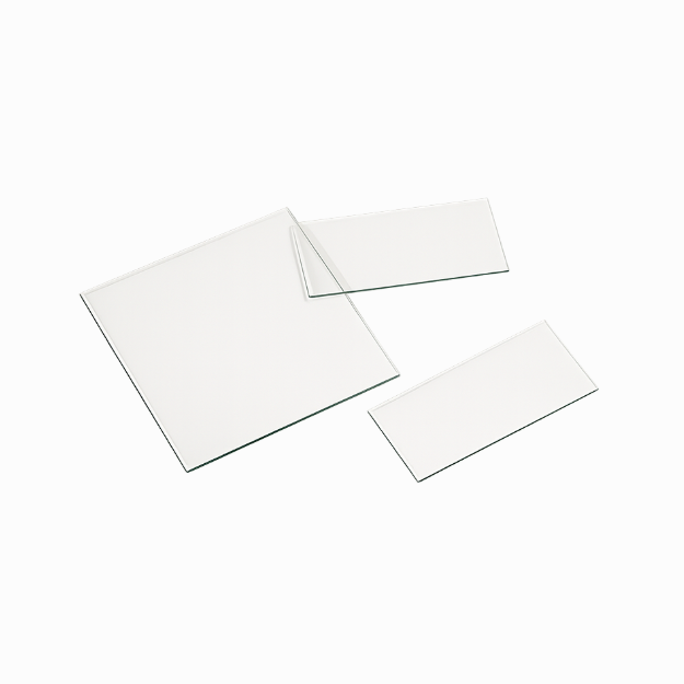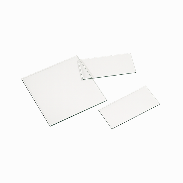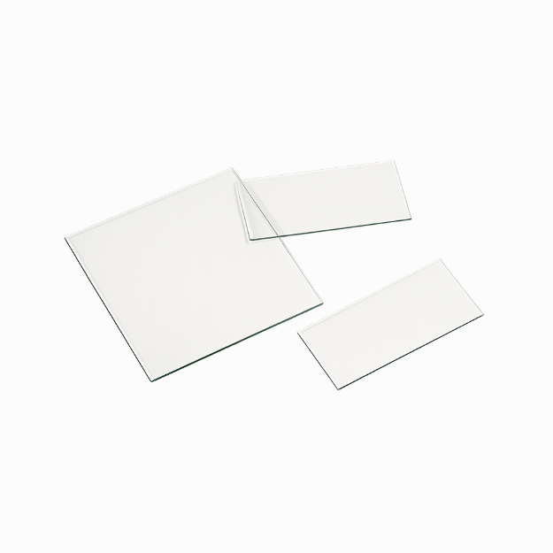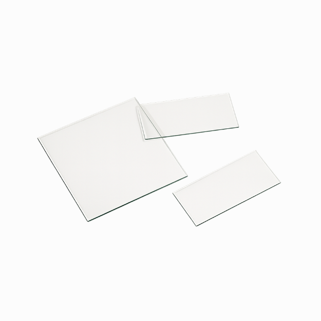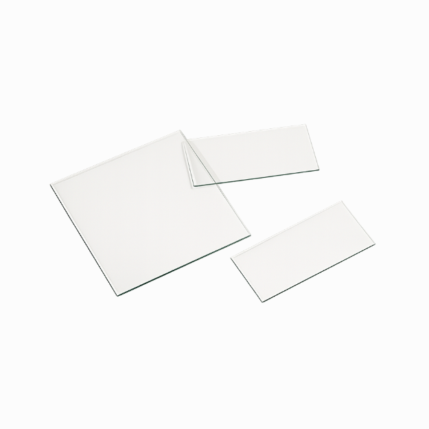
ITO CONDUCTIVE GLASS 3-4 OHM 2MM 100 PCS MAGNETRON SPUTTEREDRESEARCH GRADE MATERIAL
|
|||||||||||||||||||||||||||||||||
|
|||||||||||||||||||||||||||||||||
|
TAILORED SOLUTIONS FOR RESEARCH
Contact our engineering team for technical support or official quotations.
EMAIL: inquiry@atomfair.com
|
|||||||||||||||||||||||||||||||||
|
Manufacturer: Atomfair LLC
Brand: ATOMFAIR®
|
ITO conductive glass surfaces are susceptible to contamination from dust, grease, and organic residues. Cleaning is mandatory before use, and substrates must be handled by the edges with cleanroom-compatible tweezers and stored in a dry, dust-free environment.
- Surface Contamination Sensitivity: ITO surfaces accumulate contaminants during production, packaging, and transport, requiring mandatory cleaning before use.
- Handling Protocol: Substrates must be handled by the edges using cleanroom-compatible tweezers to avoid surface contamination.
- Storage Conditions: Unused substrates must be stored in a dry, dust-free environment to maintain surface cleanliness.
- Cleaning Requirement: Cleaning is mandatory before use; consult the provided user guidelines for detailed cleaning protocols.
Proper handling and storage of ITO conductive glass prevents surface contamination and ensures reliable performance. Follow these steps to maintain substrate cleanliness before and after use.
Required Equipment: Cleanroom-compatible tweezers
- Clean the substrate surface
Clean the ITO conductive glass surface before use according to the recommended cleaning protocol. - Handle by edges with tweezers
Handle the substrate by the edges using cleanroom-compatible tweezers to avoid surface contamination. - Store in dry dust-free environment
Store unused substrates in a dry, dust-free environment to maintain surface cleanliness.
What sheet resistance range is available for this ITO conductive glass and how does the standard 3–4 Ω/sq specification balance conductivity and optical transparency?
The square resistance can be customized from 1 Ω to 10000 Ω via magnetron sputtering. The standard 3–4 Ω/sq specification delivers excellent optical transmission with a wide bandgap and high visible-light transmittance, making it suitable for general optoelectronic applications where both conductivity and transparency are required.
What precision processing services are available to customize the shape and pattern of ITO conductive glass substrates?
Full in-house precision laser cutting, engraving, etching, hole drilling, edge grinding, polishing, ultrasonic cleaning, and coating services are available. Custom shapes include square, round, hole-drilled, slotted, and irregular workpieces, with laser lettering and pattern etching directly on the coated substrate.
What are the recommended cleaning and handling procedures for ITO conductive glass to avoid surface contamination?
Cleaning is mandatory before use as surfaces may accumulate dust, grease, and organic contaminants during production and transport. Handle substrates by the edges using cleanroom-compatible tweezers to avoid contaminating the ITO-coated side. Store unused substrates in a dry, dust-free environment.
This ITO conductive glass substrate (3–4 Ω/sq, 2 mm thick, 100 pcs) offers magnetron-sputtered indium tin oxide on multiple glass types with full customizability of resistance (1–10000 Ω) and thickness (0.05–10 mm), plus in-house laser cutting and patterning services, but requires mandatory pre-cleaning and controlled storage to avoid surface contamination.
Positive
- Broad substrate and parameter customization: Supports six substrate materials (soda-lime, borosilicate, quartz, K9, sapphire, ultra-white) with square resistance from 1 Ω to 10000 Ω and thickness from 0.05 mm to 10 mm, enabling precise matching to diverse optoelectronic and electrochemical applications.
- Integrated precision processing services: In-house laser cutting, engraving, etching, hole drilling, edge grinding, polishing, and ultrasonic cleaning allow single-source fabrication of custom geometries and patterns, eliminating multi-vendor coordination for research prototypes.
Trade-offs
- Mandatory pre-cleaning required: ITO surfaces accumulate dust, grease, and organic contaminants during production and transport; cleaning is mandatory before use, and substrates must be handled by edges with cleanroom tweezers to avoid compromising the conductive coating.
- Controlled storage environment needed: Unused substrates must be stored in a dry, dust-free environment to maintain surface cleanliness; improper storage can degrade optical transmission and electrical performance.
Every advanced material, component, equipment, and instrument in our catalog is backed by rigorous testing. We maintain strict internal quality management frameworks and align with CE conformity metrics to deliver transparent, reproducible performance data via our public open-science repository.
To request raw batch performance data, submit formal vendor registration paperwork, or execute a fast-turnaround R&D manufacturing loop, contact us at inquiry@atomfair.com.
Item is dispatched under the Atomfair Shipping & Delivery Framework (Free worldwide shipping on orders over $59 USD excl. heavy equipment). Return is governed by the Atomfair Return & Refund Policy (7-day technical return window).