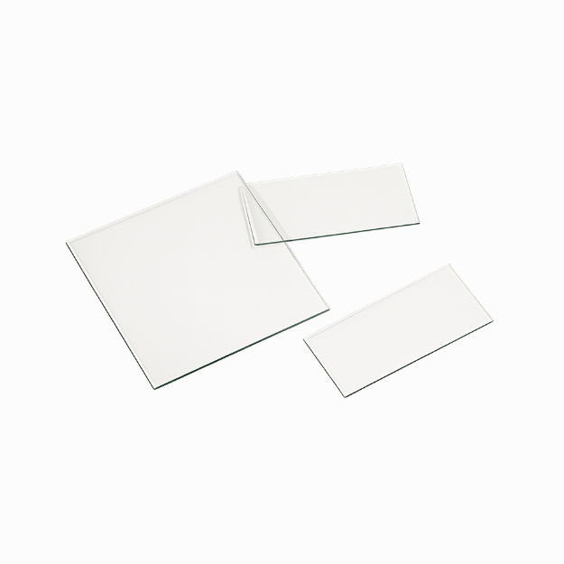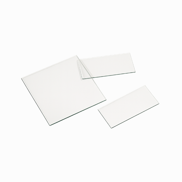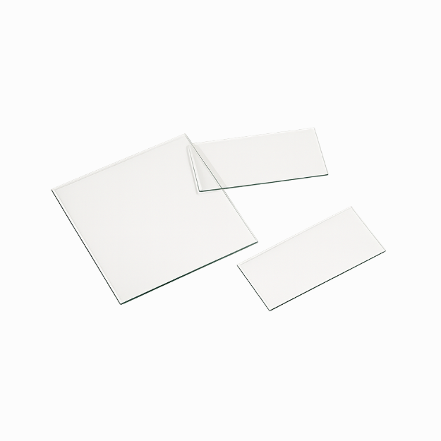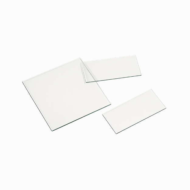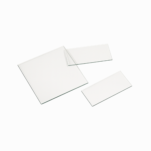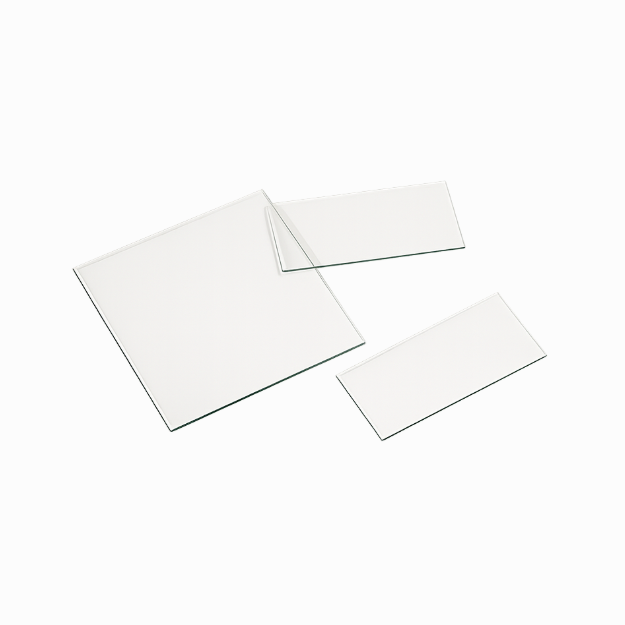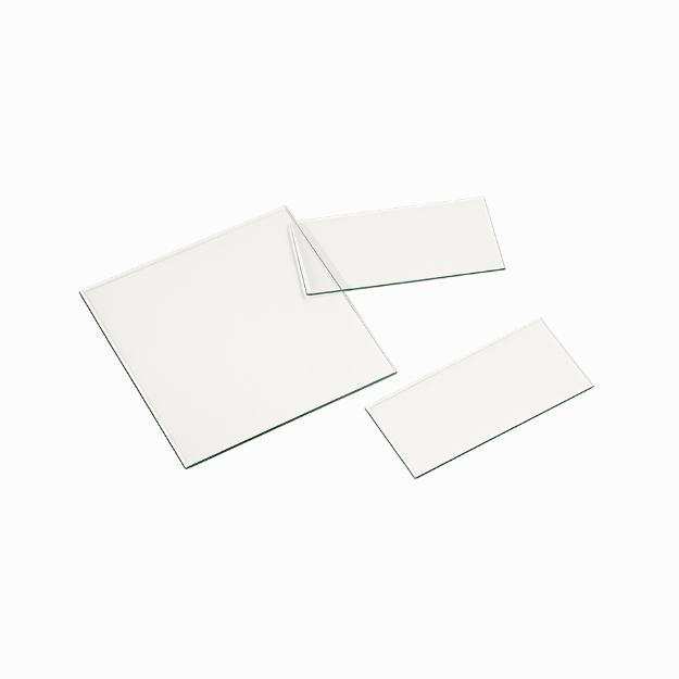
FTO CONDUCTIVE GLASS 10-15 OHM 1.1MM SNO₂:F 600°C 100 PCSRESEARCH GRADE MATERIAL
|
|||||||||||||||||||||||||||||||||||||||||||
|
|||||||||||||||||||||||||||||||||||||||||||
|
TAILORED SOLUTIONS FOR RESEARCH
Contact our engineering team for technical support or official quotations.
EMAIL: inquiry@atomfair.com
|
|||||||||||||||||||||||||||||||||||||||||||
|
Manufacturer: Atomfair LLC
Brand: ATOMFAIR®
|
The substrate requires careful handling to avoid coating damage and strict environmental storage conditions to maintain performance. Processing must account for cutting tolerances, edge treatment, and post-sintering flatness variations.
- Conductive Surface Protection: The blue film-laminated side indicates the conductive surface and must remain intact during handling to prevent scratches.
- Handling Procedure: Handle substrates only by the four edges to avoid contact with the conductive coating.
- Storage Conditions: Store in a dry, shaded location with ambient humidity below 65% to prevent degradation of sheet resistance and optical transmittance.
- CNC Processing Requirements: Custom CNC processing requires dimensional drawings and tolerance specifications to achieve ≤0.05 mm cutting precision.
- Post-Sintering Flatness Consideration: Account for post-sintering surface flatness values of 3.375 μm and 11.225 μm in device architectures requiring precise layer thickness control.
Follow these steps to safely handle and store FTO conductive glass substrates while preserving coating integrity. Proper handling prevents scratches and environmental damage that degrade electrical and optical performance.
- Identify the conductive surface
Identify the conductive surface by locating the blue film-laminated side of the substrate. - Handle by edges only
Handle the substrate by gripping only the four edges and avoiding contact with the conductive coating. - Store in controlled environment
Store the substrate in a dry, shaded location with ambient humidity below 65% to prevent degradation of sheet resistance and optical transmittance. - Avoid impact damage
Handle the substrate gently to avoid impact with hard tooling or equipment surfaces.
Why is FTO conductive glass preferred over ITO for dye-sensitized solar cell fabrication requiring high-temperature sintering?
FTO (SnO₂:F) conductive glass withstands operating temperatures up to 600°C, whereas ITO degrades above 300°C. This thermal stability enables high-temperature sintering of mesoporous TiO₂ layers in dye-sensitized solar cells without loss of conductivity. Additionally, the fluorine-doped tin oxide coating exhibits superior room-temperature acid corrosion resistance, making it suitable for acidic electrolytes that would etch ITO coatings.
How do the pre-sinter and post-sinter surface flatness values of FTO glass affect device fabrication?
The product specification lists pre-sinter surface flatness as 1.225 μm / 9.287 μm and post-sinter flatness as 3.375 μm / 11.225 μm. These values must be considered in device architectures requiring precise layer thickness control, as thermal processing can increase surface roughness and impact subsequent thin-film deposition uniformity.
What are the critical handling and storage requirements for FTO conductive glass to maintain performance?
Handle FTO substrates only by the four edges to avoid touching the conductive coated surface. The blue film-laminated side identifies the conductive surface; verify orientation before use. For long-term storage, maintain ambient humidity below 65% in a dry, shaded location away from direct sunlight to prevent degradation of sheet resistance and optical transmittance.
This FTO conductive glass (SnO₂:F, 10–15 Ω/sq, 350 nm coating on 1.1 mm substrate) offers 600°C thermal stability and acid resistance, making it the preferred transparent electrode for dye-sensitized solar cell sintering and photoelectrochemical experiments where ITO degrades. Individual blue-film lamination protects the conductive surface and aids orientation.
Positive
- 600°C High-Temperature Stability: The SnO₂:F coating remains stable up to 600°C, enabling high-temperature sintering of mesoporous TiO₂ layers in dye-sensitized solar cell fabrication and thermal catalytic experiments where ITO would fail above 300°C.
- Superior Acid and Chemical Resistance: The fluorine-doped tin oxide coating exhibits outstanding room-temperature resistance to acid corrosion, making it the substrate of choice for photoelectrochemical experiments involving acidic electrolytes that would etch ITO coatings.
Trade-offs
- Strict Handling and Storage Requirements: Substrates must be handled by edges only to avoid coating damage; the blue film side indicates the conductive surface. Long-term storage requires ambient humidity below 65% in a dry, shaded location to prevent degradation of sheet resistance and optical transmittance.
- Post-Sintering Surface Flatness Variation: Post-sintering surface flatness values (3.375 μm / 11.225 μm) must be accounted for in device architectures requiring precise layer thickness control, as flatness degrades from pre-sinter values.
Every advanced material, component, equipment, and instrument in our catalog is backed by rigorous testing. We maintain strict internal quality management frameworks and align with CE conformity metrics to deliver transparent, reproducible performance data via our public open-science repository.
To request raw batch performance data, submit formal vendor registration paperwork, or execute a fast-turnaround R&D manufacturing loop, contact us at inquiry@atomfair.com.
Item is dispatched under the Atomfair Shipping & Delivery Framework (Free worldwide shipping on orders over $59 USD excl. heavy equipment). Return is governed by the Atomfair Return & Refund Policy (7-day technical return window).