|
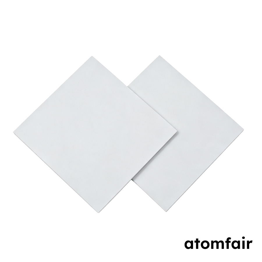
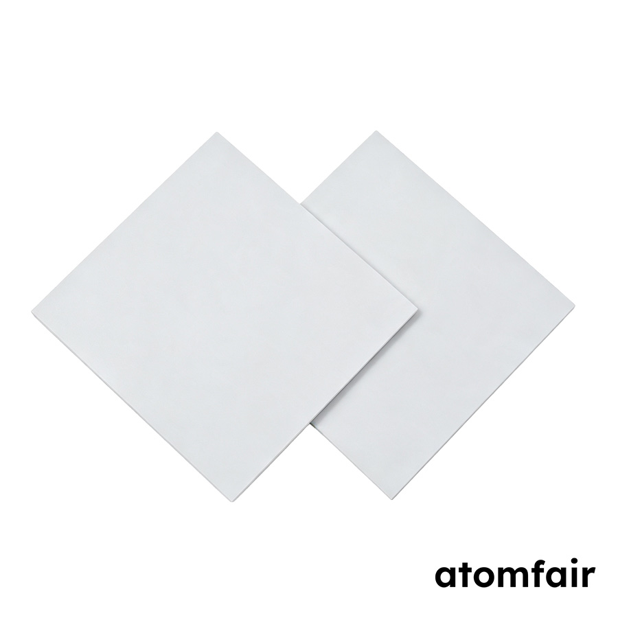
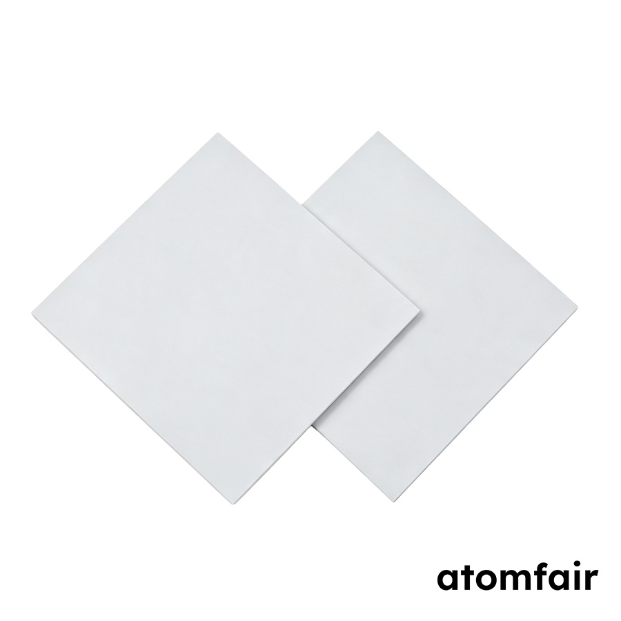
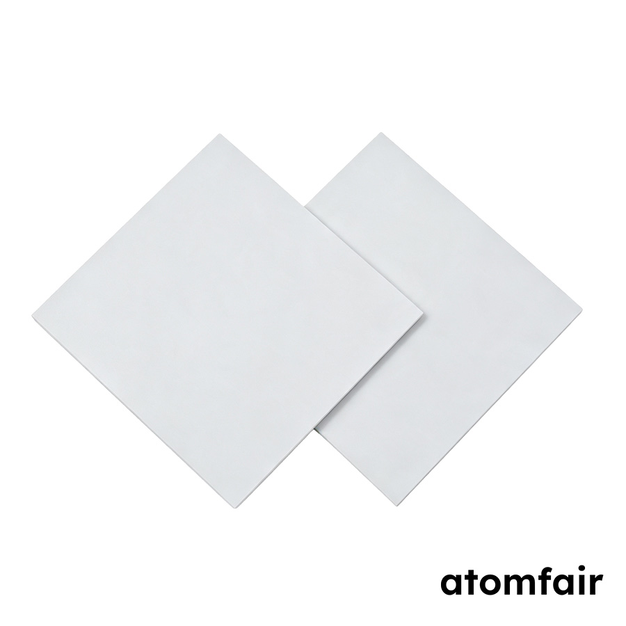
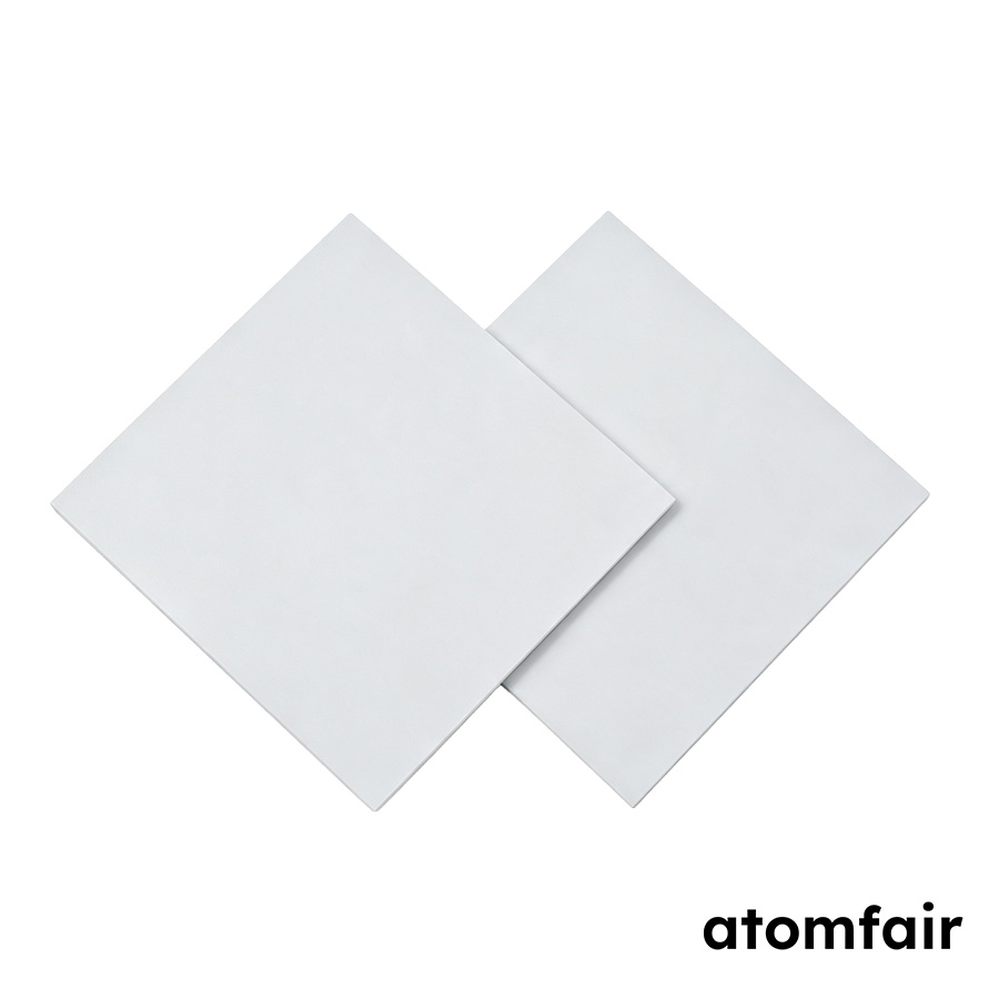
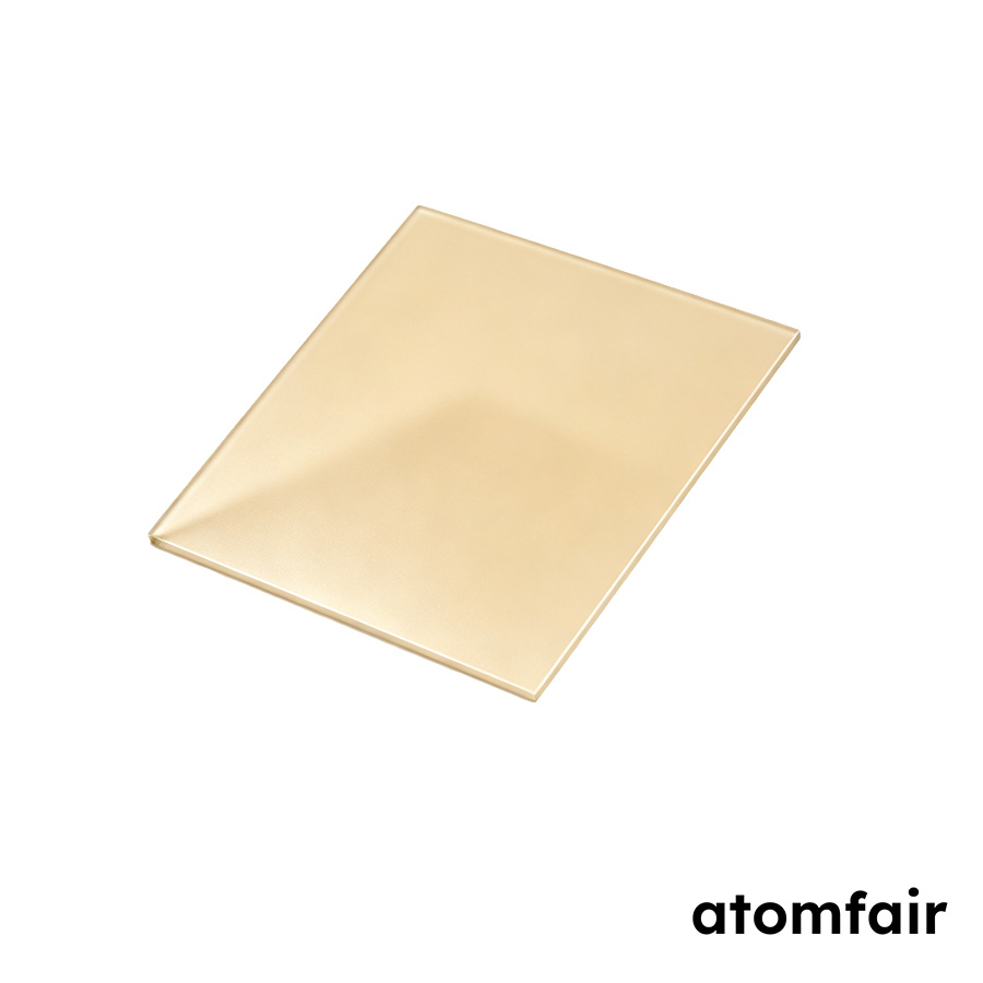
Gadolinium Gallium Garnet Single Crystal Substrate, (100), DSP (10 pcs/box)
Product Type: GGG single crystal substrate
Research-grade laboratory product
|
|||||||||||||||||||||||||||||||||||||||||||||||
|
|||||||||||||||||||||||||||||||||||||||||||||||
|
LABORATORY PROCUREMENT SUPPORT
For material matching, specification review, model selection or configuration confirmation, contact our technical sales team.
E-MAIL: inquiry@atomfair.com
|
|||||||||||||||||||||||||||||||||||||||||||||||
|
Manufacturer: Atomfair LLC
Brand: ATOMFAIR®
|
This substrate requires material and crystal family matching to the target thin-film workflow. Orientation (100) and double-side polished surface finish must be verified before use.
- Material Matching: Confirm that the selected substrate material and crystal family match the target thin-film or device workflow before quotation.
- Specification Review: Verify orientation, dimensions, thickness, polishing condition, offcut details, quantity, and any custom requirements for the selected option.
What is the lattice constant of the GGG (100) substrate and how does it affect thin-film epitaxy?
The GGG (100) substrate has a lattice constant of a = 12.380 Å (cubic, Z=8). This value is a critical parameter for assessing lattice mismatch with deposited thin-film materials, influencing epitaxial quality and defect density. The product description provides this lattice constant, allowing researchers to evaluate compatibility with their target material system.
What does DSP surface finish mean for GGG substrates and what are its advantages for thin-film deposition?
DSP stands for double-side polished. The product is specified with a DSP surface finish, which provides a smooth, planar surface on both sides of the substrate. This minimizes scattering and improves film uniformity, which is essential for high-quality thin-film deposition and device fabrication.
How does the Czochralski growth method used for this GGG substrate affect its crystal quality?
The GGG substrate is grown by the Czochralski method (CZ), which produces high-purity (99.99%), single-crystal boules with low dislocation density and uniform lattice constant. This growth method is standard for producing large-area, high-quality substrates for epitaxial growth of thin films.
The GGG (100) double-side polished substrate provides a high-purity (99.99%) cubic template with a lattice constant of 12.380Å, suitable for garnet-based epitaxy. Its thin 0.5 mm thickness and limited size options impose handling and material-matching constraints.
Positive
- High purity 99.99%: With 99.99% purity, this substrate minimizes impurity-induced defects during thin-film deposition, critical for high-quality epitaxial layers.
- High melting point 1750-1800°C: The melting point exceeds 1750°C, allowing thermal processing steps such as annealing or high-temperature growth without substrate degradation.
Trade-offs
- Material matching required: The substrate must be matched to the target thin-film material and crystal family to avoid lattice mismatch or thermal expansion incompatibility.
- Fixed thin substrate dimensions: Only two size options (5×5 and 10×10 mm) with 0.5 mm thickness are available, limiting flexibility for non-standard device geometries.
Every advanced material, component, equipment, and instrument in our catalog is backed by rigorous testing. We maintain strict internal quality management frameworks and align with CE conformity metrics to deliver transparent, reproducible performance data via our public open-science repository.
To request raw batch performance data, submit formal vendor registration paperwork, or execute a fast-turnaround R&D manufacturing loop, contact us at inquiry@atomfair.com.
Item is dispatched under the Atomfair Shipping & Delivery Framework (Free worldwide shipping on orders over $59 USD excl. heavy equipment). Return is governed by the Atomfair Return & Refund Policy (7-day technical return window).