
Epitaxial Wafers & Semiconductor Thin Films
Epitaxial wafers and semiconductor thin films are essential materials for semiconductor devices, optoelectronics, power electronics, sensors, MEMS, and advanced materials research. This category brings together semiconductor wafers with controlled epitaxial layers, compound semiconductor epitaxial wafers, two-dimensional semiconductor films, dielectric films, oxide and nitride films, as well as metal and functional coated substrates.
Products can be selected according to material system, substrate type, crystal orientation, epitaxial or film thickness, doping type, resistivity, wafer size, surface roughness, and single-sided or double-sided configuration. Whether you need an epitaxial wafer for device fabrication, a compound semiconductor platform for optoelectronic research, or a thin-film substrate for sensing, flexible electronics, or nanodevice development, the material structure should be matched to the intended application and process.
Use the selection guide below to compare material families, substrate structures, film types, and key specification priorities before choosing a wafer or thin-film platform.
Show More: Explore Epitaxial Wafers and Semiconductor Thin Films
Semiconductor Epitaxial Wafers
Silicon epitaxial wafers are used for device prototyping, junction structures, power devices, detectors, integrated-circuit process development, and laboratory fabrication. Products can be selected according to epitaxial-layer structure, conductivity type, doping level, crystal orientation, and substrate resistivity.
| Selection Factor | Common Options |
|---|---|
| Material system | Silicon, germanium, and other semiconductor systems |
| Epitaxial structure | Single-layer, multilayer, or engineered epitaxial structures |
| Conductivity type | N-type, P-type, or undoped |
| Doping level | Lightly doped, moderately doped, or heavily doped |
| Crystal orientation | <100>, <110>, <111>, or application-specific orientations |
| Layer thickness | Selected according to junction depth, isolation, or device design |
| Substrate | Conductive, high-resistivity, or application-specific silicon |
| Wafer size | Research-scale and larger wafer formats |
Compound Semiconductor Epitaxial Wafers
Compound semiconductor epitaxial wafers provide electronic, optical, thermal, and high-frequency properties that differ from silicon. They are widely used for LEDs, lasers, photodetectors, RF devices, high-electron-mobility structures, and wide-bandgap power electronics.
Common material families include GaAs and AlGaAs, InP and InGaAs, GaN and AlGaN/GaN, InGaN, 4H-SiC, and other III-V or compound semiconductor systems. When selecting a compound semiconductor wafer, review the substrate material, lattice matching, buffer layer, active-layer composition, strain management, carrier concentration, and intended wavelength or operating voltage.
Two-Dimensional Semiconductor Thin Films
Two-dimensional semiconductor films are used for optoelectronics, flexible electronics, nanoelectronics, chemical sensing, biosensing, and emerging device architectures. Depending on the application, films may be supplied as monolayer, few-layer, multilayer, continuous, or transfer-compatible structures.
Representative material families include MoS2, WS2, WSe2, MoSe2, h-BN, graphene, and other transition-metal dichalcogenides.
| Application Requirement | Suitable Direction |
|---|---|
| Strong monolayer optical or electronic behavior | Monolayer or few-layer films |
| Greater thickness or process robustness | Multilayer films |
| Direct device fabrication | Film supplied on a defined substrate |
| Flexible or transparent devices | Transfer-compatible films |
| Large-area process development | Larger wafer-format films |
| Specific electrical behavior | Confirm layer count, doping, grain structure, and substrate |
Oxide, Nitride, and Dielectric Thin Films
Dielectric and insulating films are used for electrical isolation, gate structures, passivation, optical interfaces, MEMS fabrication, and multilayer device construction. Common systems include SiO2, silicon nitride, Al2O3, high-k dielectrics, oxynitrides, and engineered multilayer stacks.
Important selection factors include film thickness and uniformity, dielectric strength, refractive index, surface roughness, film stress, pinhole control, deposition method, and compatibility with lithography, etching, annealing, or bonding.
Metal and Functional Thin Films
Metal and functional coatings are used for electrodes, conductive contacts, diffusion barriers, catalytic interfaces, sensor surfaces, and optoelectronic structures. Common systems include Au, Cr/Au, Pt, Ti/Pt, Al, Cu, and other customized metal stacks.
| Application Priority | Selection Direction |
|---|---|
| Conductive contacts and microelectrodes | Gold, aluminum, copper, or metal stacks |
| Chemical stability and electrochemical use | Platinum or Ti/Pt systems |
| Improved film adhesion | Titanium, chromium, or other adhesion layers |
| Optical or plasmonic research | Low-roughness noble-metal films |
| High-temperature or demanding environments | Temperature-resistant and corrosion-resistant film systems |
| Two-sided device structures | Double-sided deposition or coating |
Substrate and Wafer Configurations
The substrate directly affects the electrical, optical, thermal, and processing performance of a thin-film platform. Common configurations include silicon wafers, oxidized silicon wafers, silicon nitride wafers, glass, quartz, sapphire, conductive substrates, high-resistivity substrates, single-sided coated substrates, double-sided coated substrates, and customized substrate dimensions.
For optical, transparent, flexible, or high-temperature applications, confirm the required transparency, insulation, conductivity, thermal stability, surface treatment, and compatibility with transfer or subsequent processing.
How to Choose the Right Product
| Primary Requirement | Recommended Direction |
|---|---|
| Controlled crystalline semiconductor layer | Silicon epitaxial wafer or compound semiconductor epitaxial wafer |
| RF or optoelectronic device development | GaAs, InP, GaN, or related compound semiconductor platform |
| Wide-bandgap power-device research | GaN, AlGaN/GaN, or SiC epitaxial wafer |
| Two-dimensional material devices | MoS2, WS2, WSe2, graphene, or related thin film |
| Electrical isolation or gate dielectric | SiO2, silicon nitride, Al2O3, or another dielectric film |
| Electrode or conductive interface | Au, Cr/Au, Pt, Ti/Pt, or another conductive film |
| Flexible-device development | Transfer-compatible film or film on a flexible substrate |
| Optical-device fabrication | Low-roughness, optically suitable substrate and film |
| High-temperature or chemical processing | Thermally stable substrate and corrosion-resistant film system |
| Large-area process development | Large-format wafer and uniform thin-film platform |
Before ordering, confirm the material system, wafer diameter, substrate type, crystal orientation, conductivity type, resistivity, epitaxial or film thickness, doping requirement, surface roughness, single-sided or double-sided configuration, and required quantity. For customized structures, also provide the intended application and processing conditions so the wafer or film can be matched to the device design.
Frequently Asked Questions
What is an epitaxial wafer?
An epitaxial wafer is a semiconductor substrate with one or more controlled crystalline layers grown in a defined orientation. The epitaxial layer can be selected by material, thickness, doping type, resistivity, and device function.
How is a thin film different from an epitaxial layer?
An epitaxial layer normally maintains a defined crystallographic relationship with the substrate. A thin film may be single-crystalline, polycrystalline, amorphous, or layered, and may be produced by CVD, PVD, evaporation, sputtering, PECVD, ALD, or other deposition methods.
How should I choose between silicon, GaAs, InP, GaN, and SiC?
Silicon is suitable for many general device and process-development applications. GaAs and InP are widely used for optoelectronic and high-frequency devices. GaN is commonly selected for high-frequency, high-voltage, and high-power applications, while SiC is often used for high-temperature, high-voltage, and high-power environments. The final choice should also consider the device structure, operating wavelength, voltage, and fabrication process.
What is the difference between monolayer and multilayer films?
Monolayer and few-layer films are often chosen to study the optical, electronic, and interfacial properties of two-dimensional materials. Multilayer films generally provide greater thickness and process robustness. The appropriate choice depends on the device structure, transfer method, and subsequent processing requirements.
How do I choose the correct film thickness?
Film thickness affects conductivity, optical transmission, dielectric performance, surface morphology, and mechanical stability. Optical, surface-sensitive, and two-dimensional-material applications often require thinner films, while isolation layers, electrodes, and mechanically robust structures may require thicker films.
Should I choose a single-sided or double-sided film?
Choose a single-sided configuration when the rear surface is needed for handling, mounting, heat transfer, optical access, or subsequent processing. Choose a double-sided configuration when both surfaces must provide electrical, optical, or functional performance.
Can the substrate be selected separately from the film?
The substrate is often an integral part of a thin-film platform. Silicon, oxidized silicon, silicon nitride, glass, quartz, sapphire, conductive substrates, and flexible substrates provide different electrical, optical, thermal, and processing characteristics. Selection should be based on the final application.
What information should I provide when requesting a quotation?
Provide the material system, substrate type, wafer size, crystal orientation, conductivity type or resistivity, epitaxial or film thickness, doping requirement, surface roughness, single-sided or double-sided configuration, quantity, and intended application. These details help match the product to your device design and fabrication process.
Showing 17–32 of 46 results
-
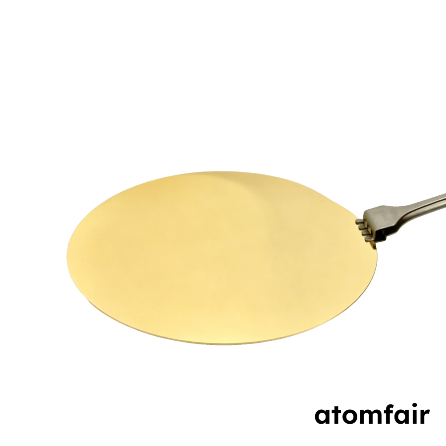
Gold-Coated Substrate 2 Inch Cr/Au 30/100 nm ATOMFAIR®
$76.00 -
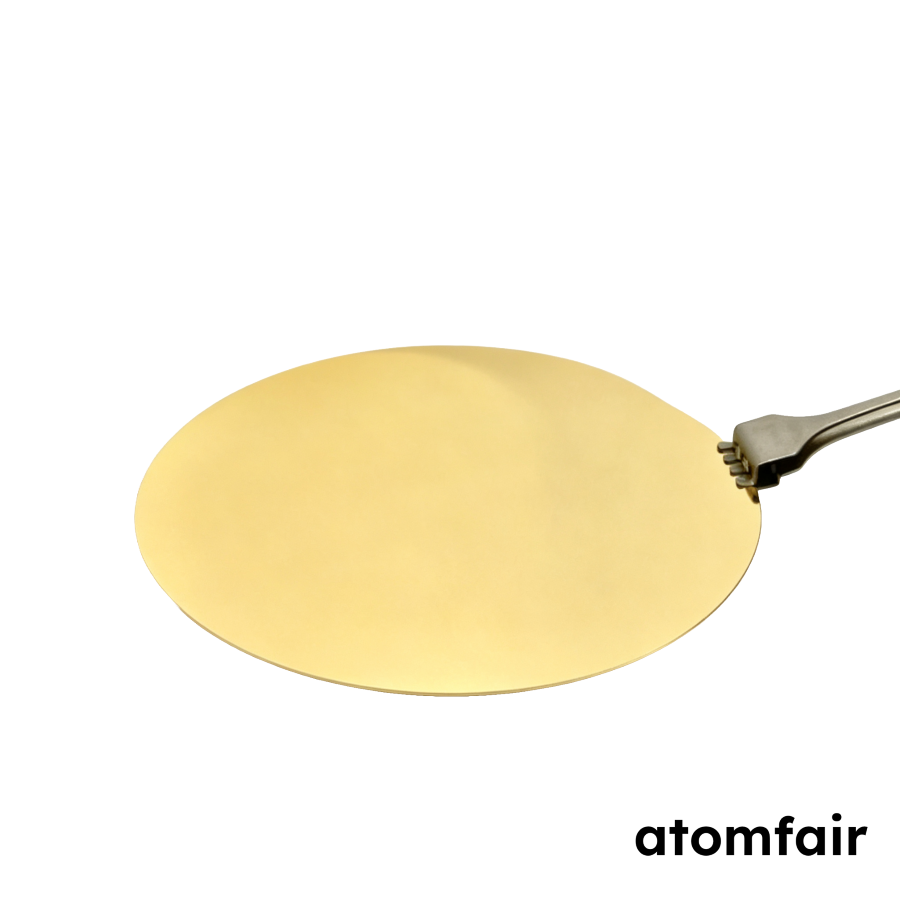
Gold-Coated Substrate 2 Inch Cr/Au Double-Sided ATOMFAIR®
$103.00 -
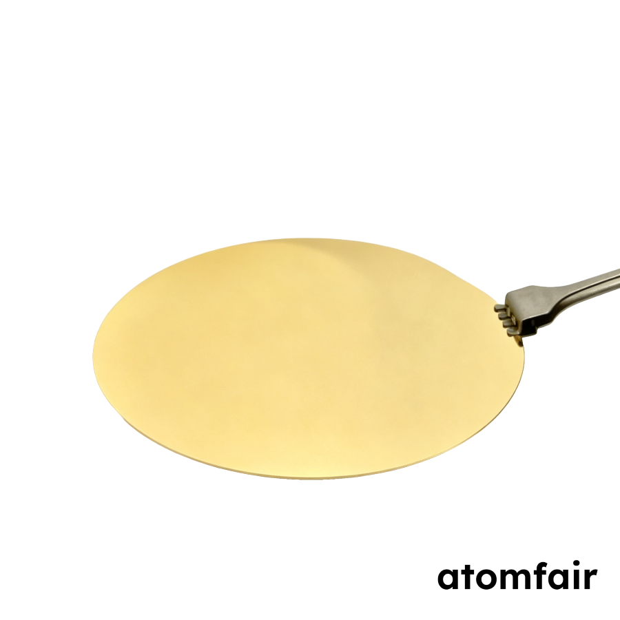
Gold-Coated 4 Inch Substrate Cr/Au 30/100 nm ATOMFAIR®
$138.00 -
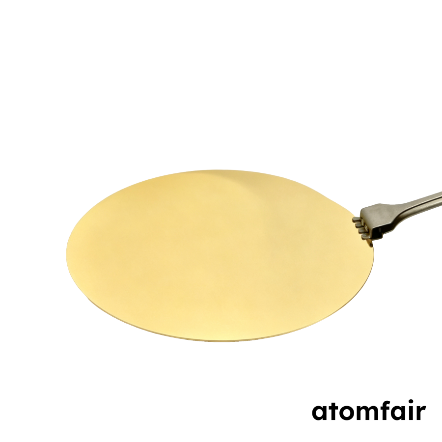
Gold-Coated Substrate Cr/Au 4 Inch Double-Sided ATOMFAIR®
$191.00 -
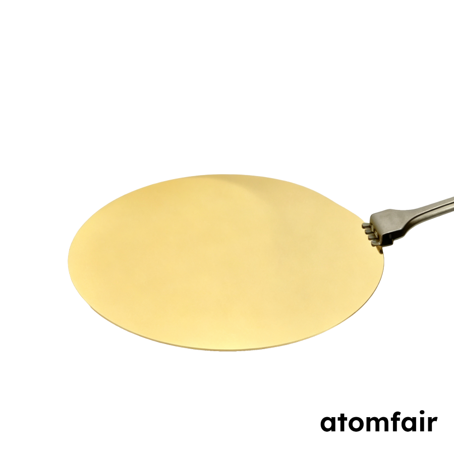
Gold-Coated 6 Inch Substrate Cr/Au 30/100 nm ATOMFAIR®
$227.00 -
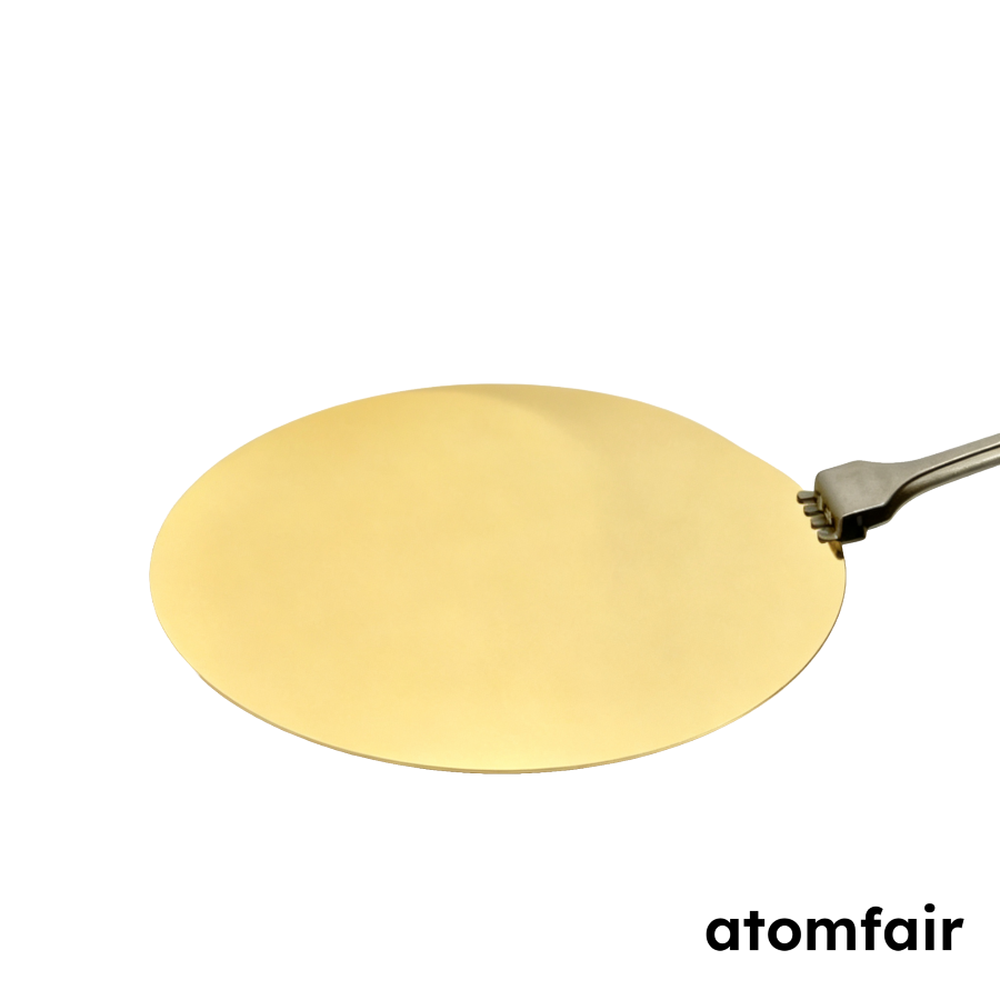
Gold-Coated Substrate 6 Inch Cr 30 nm/Au 100 nm ATOMFAIR®
$315.00 -
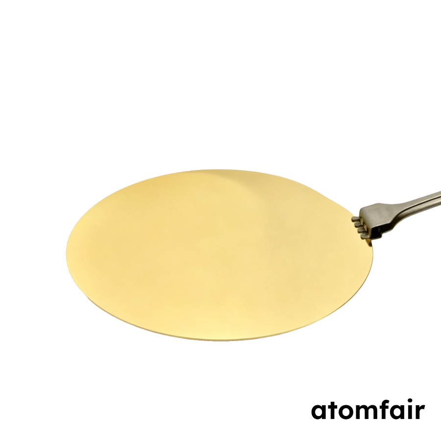
Gold-Coated Substrate 8 in Cr/Au 30/100 nm ATOMFAIR®
$333.00 -
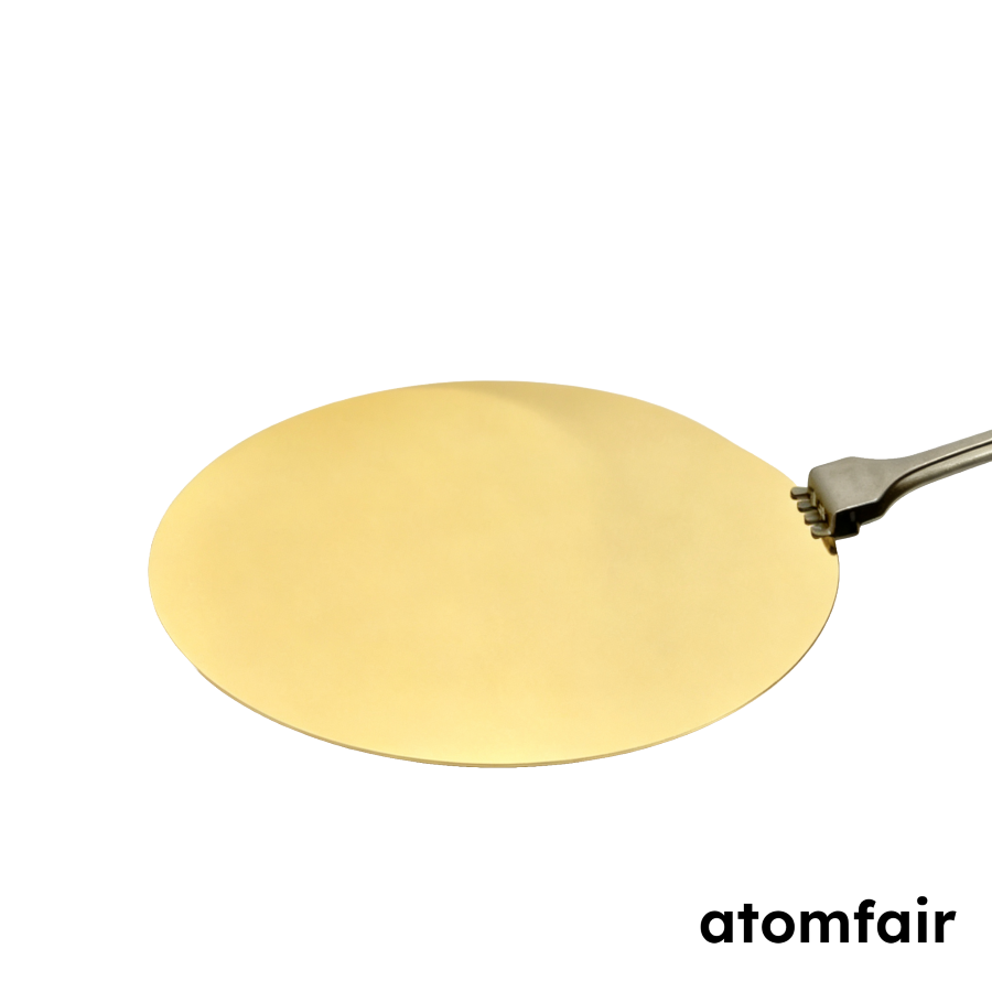
Gold-Coated Substrate 8 Inch Cr/Au Double-Sided ATOMFAIR®
$60.00 -
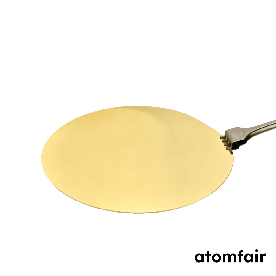
Gold-Coated 12 Inch Substrate Cr 30 nm/Au 100 nm ATOMFAIR®
$634.00 -
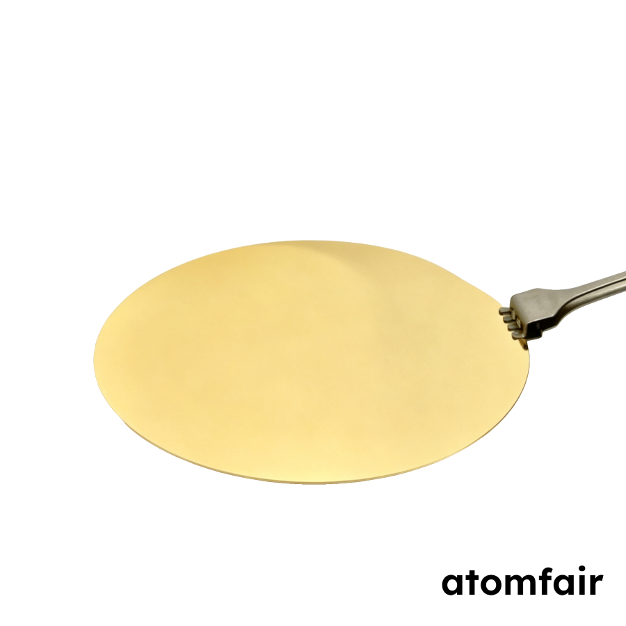
Gold-Coated Substrate Cr30/Au100 12 Inch Ra<1nm ATOMFAIR®
$899.00 -
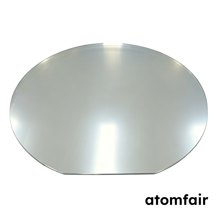
Platinum-Coated Substrate 2 in Ti/Pt Stack ATOMFAIR®
$67.00 -
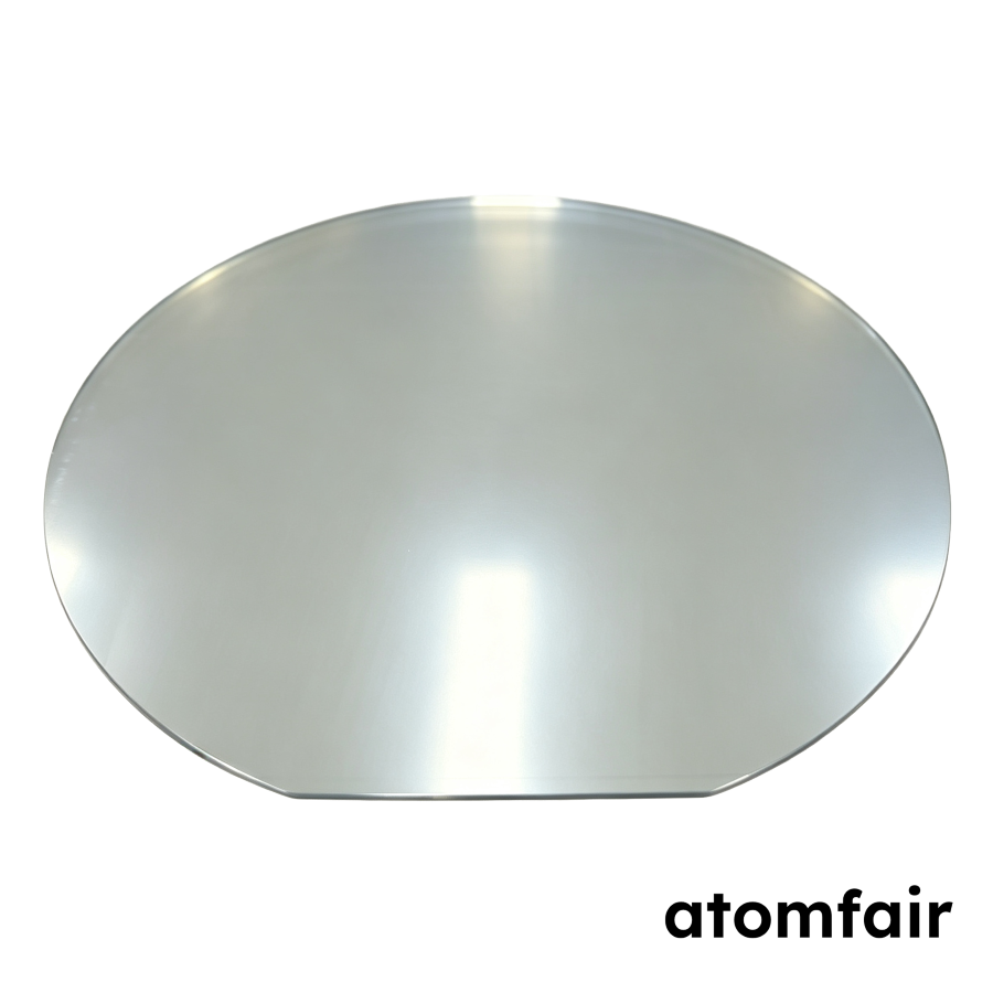
Platinum-Coated Substrate 2 in Ti/Pt Double-Sided ATOMFAIR®
$94.00 -
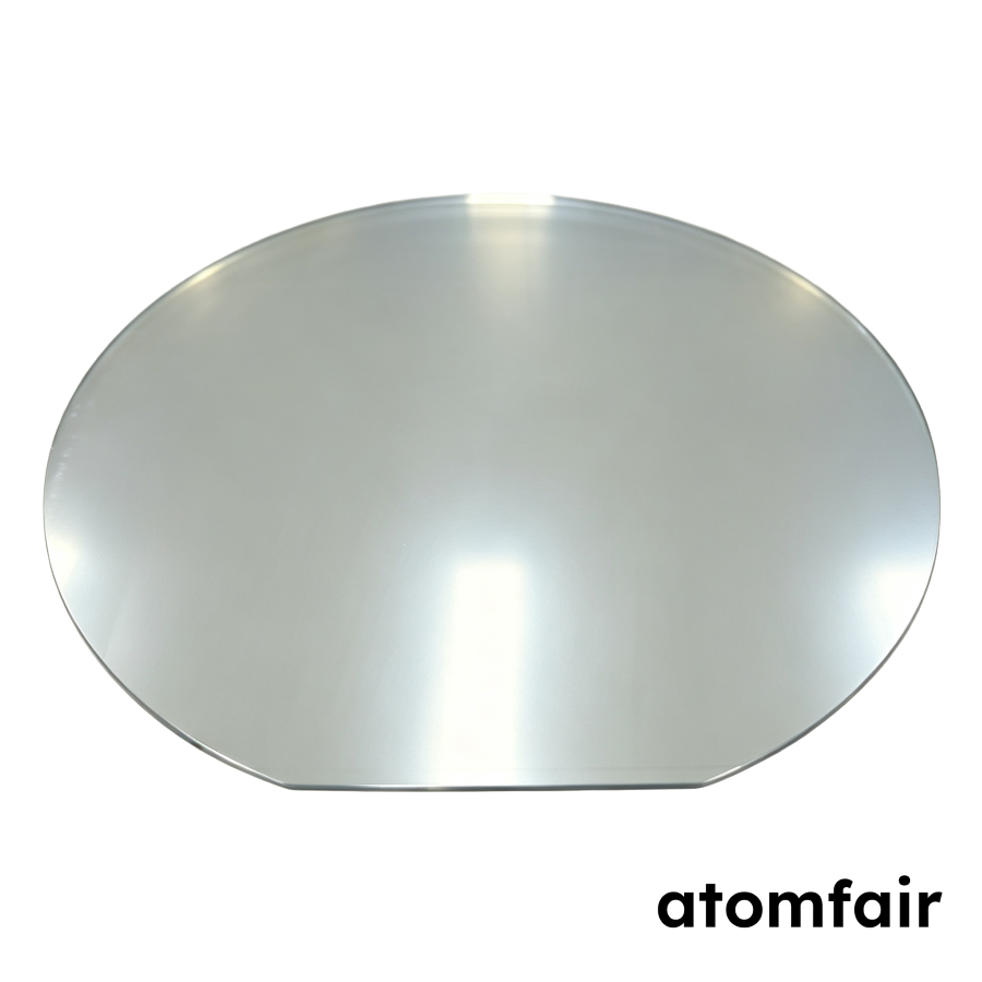
Platinum-Coated 4 Inch Substrate Ti/Pt 30/100 nm ATOMFAIR®
$94.00 -
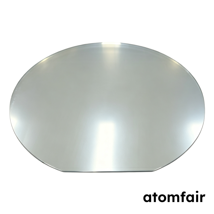
Double-Sided Platinum-Coated 4 Inch Substrate ATOMFAIR®
$138.00 -
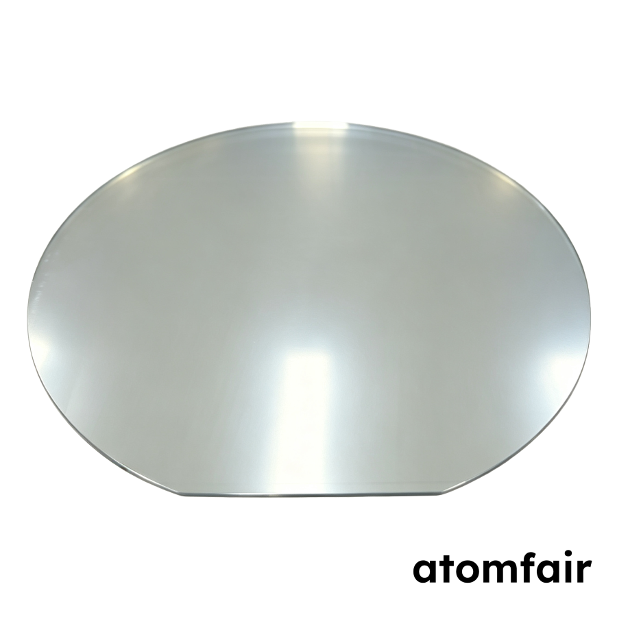
Platinum-Coated 6 Inch Substrate Ti/Pt Stack ATOMFAIR®
$138.00 -
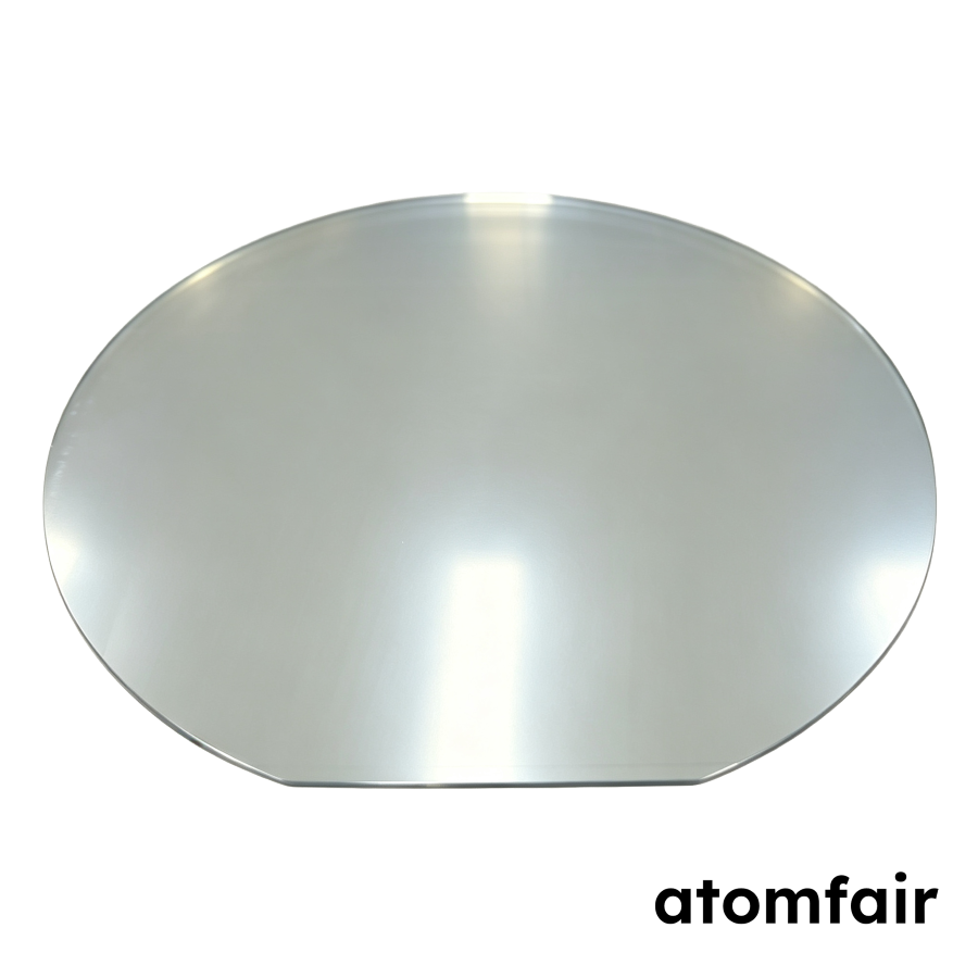
Platinum-Coated 6 Inch Substrate Ti/Pt 30/100 nm ATOMFAIR®
$209.00