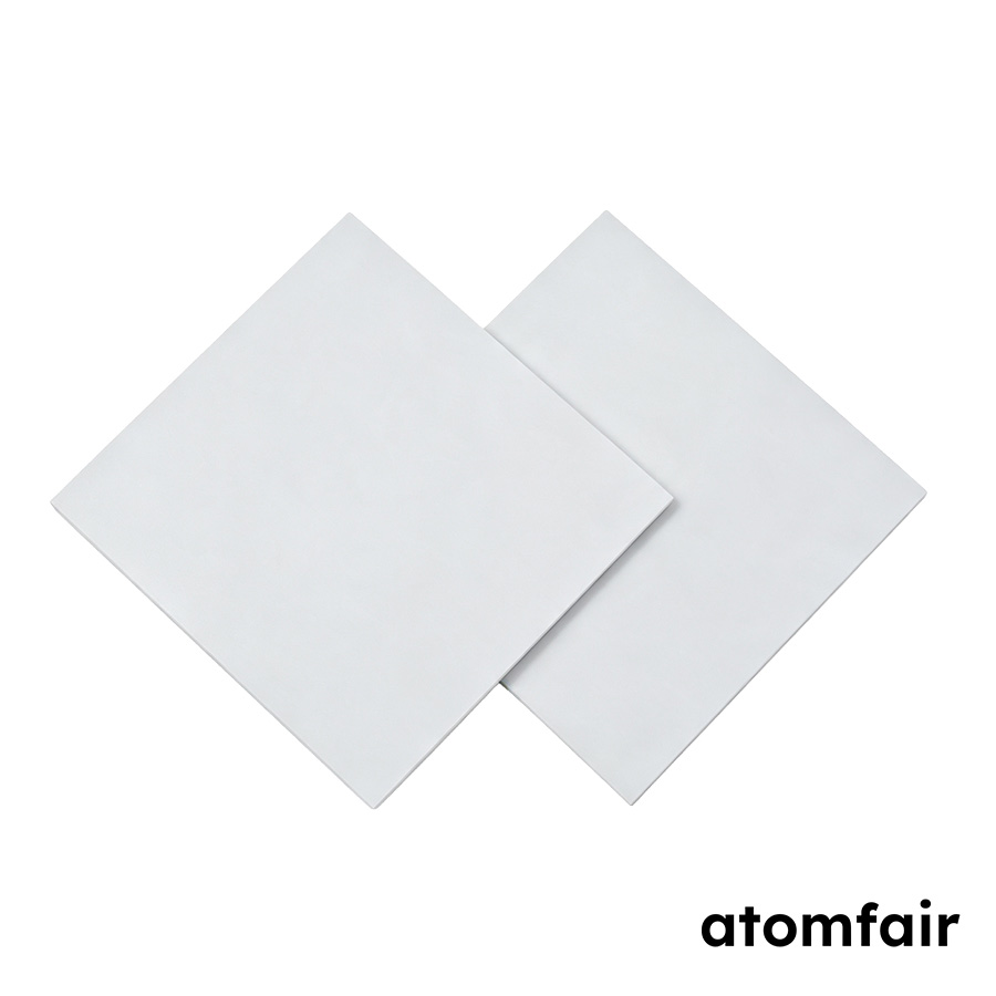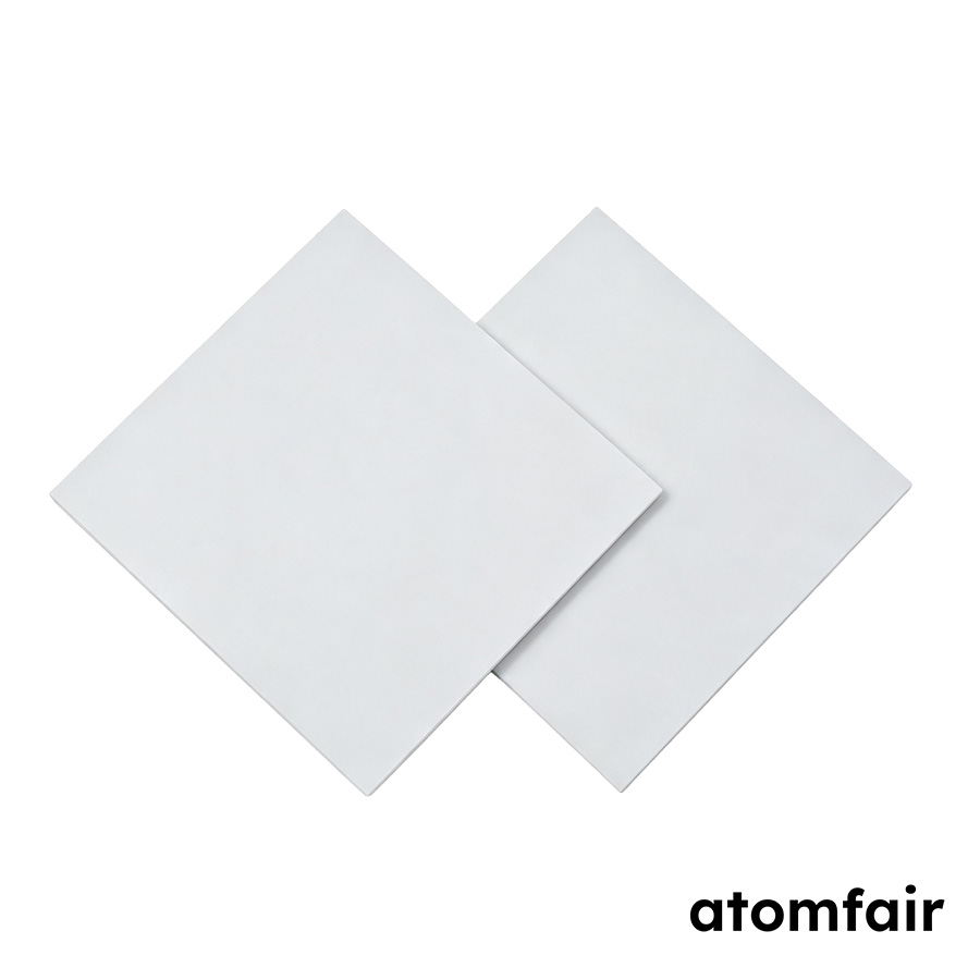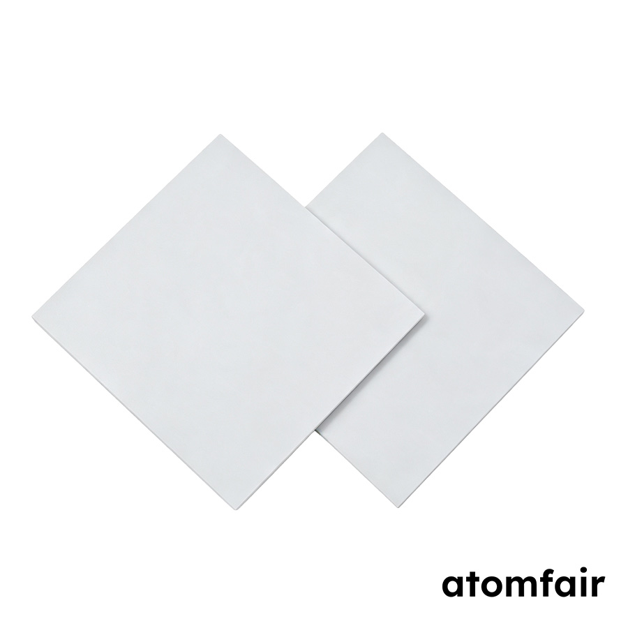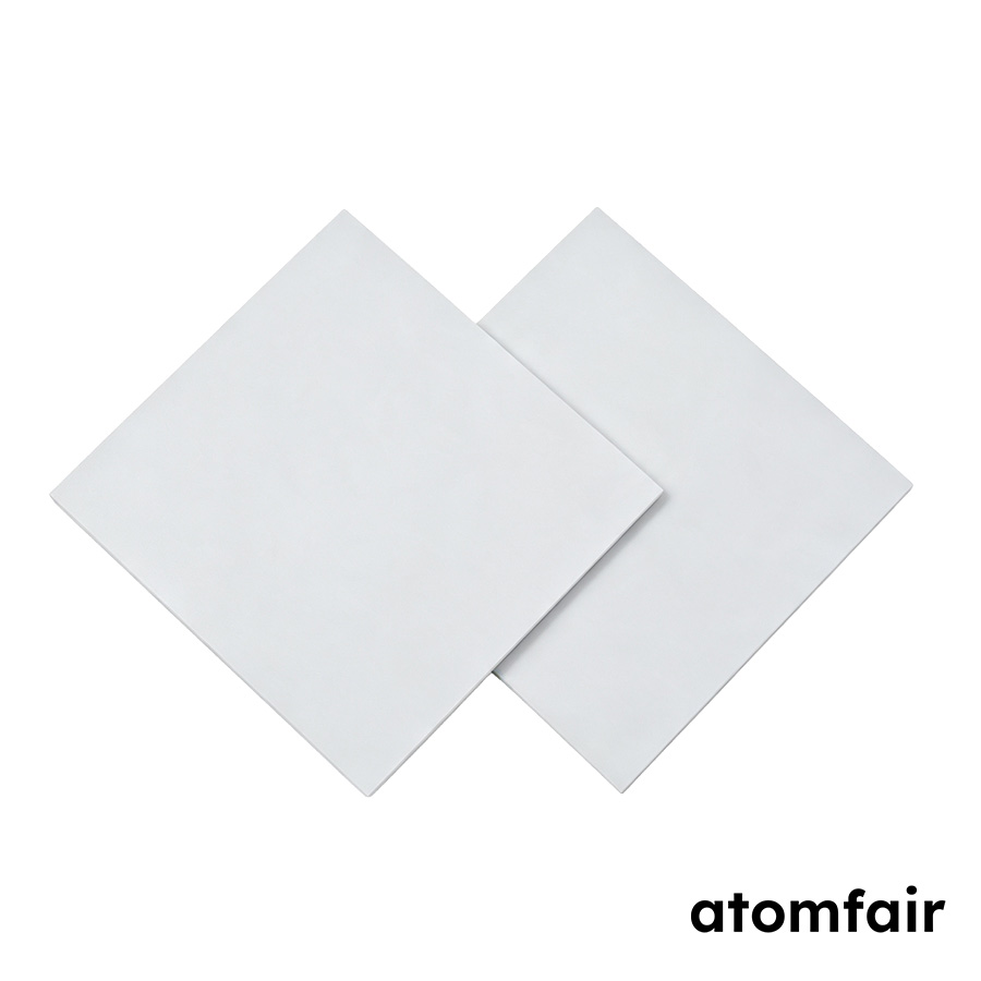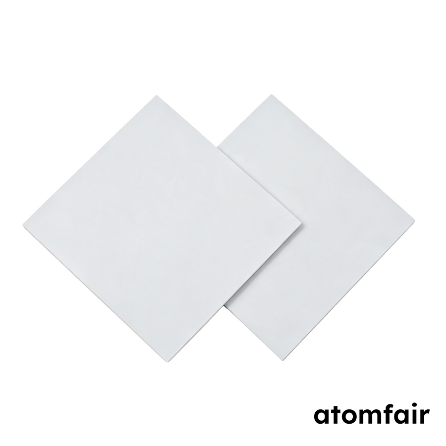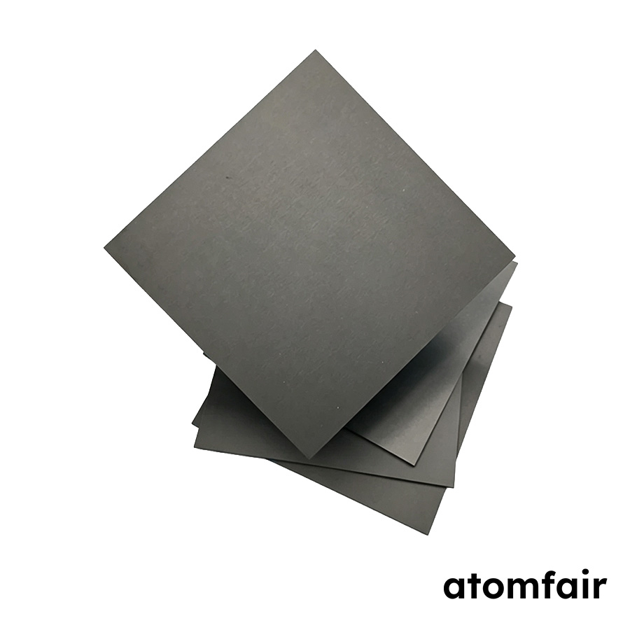
Silicon Nitride Ceramic Substrate, 114 mm x 114 mm x 0.32 mmProduct Type: Technical ceramic substrate
Research-grade laboratory product
|
|||||||||||||||||||||||||||||||||
|
|||||||||||||||||||||||||||||||||
|
LABORATORY PROCUREMENT SUPPORT
For model selection, accessory matching, platform compatibility or configuration confirmation, contact our technical sales team.
E-MAIL: inquiry@atomfair.com
|
|||||||||||||||||||||||||||||||||
|
Supplier: Atomfair
Brand: ATOMFAIR®
|
What is the maximum operating temperature and thermal conductivity of this 114 mm x 114 mm x 0.32 mm silicon nitride substrate?
This silicon nitride ceramic substrate has a usable temperature range from -55 °C to 850 °C and a thermal conductivity above 60 W/(m·K). These specifications make it suitable for high-temperature and high-power applications requiring efficient heat dissipation and structural integrity.
Can this substrate be ordered with metallization or custom surface finishes for direct bonding applications?
Yes, this substrate supports optional configuration for polishing, coating, metallization, or custom shaping as required for the application. Buyers should confirm these needs with the technical sales team to ensure compatibility with downstream processes such as active metal brazing or direct bonded copper.
What mechanical and electrical performance thresholds does this 0.32 mm thick silicon nitride substrate provide for demanding environments?
This substrate delivers flexural strength above 600 MPa, fracture toughness of 6.5 MPa·√m, Young's modulus above 310 GPa, Vickers hardness above 15 GPa, and breakdown voltage above 15 kV/mm. These properties ensure mechanical robustness and electrical insulation under high stress and thermal cycling conditions.
This 114 mm x 114 mm x 0.32 mm silicon nitride ceramic substrate offers a flexural strength >600 MPa and thermal conductivity >60 W/(m·K), enabling use as a structural and thermal management component in high-stress laboratory setups, though its brittle nature and moderate breakdown voltage impose handling and dielectric constraints.
Positive
- High mechanical strength and toughness: Flexural strength >600 MPa and fracture toughness 6.5 MPa√m provide reliable mechanical integrity under load, suitable for structural substrates in demanding environments.
- Broad temperature range usability: Operable from -55 °C to 850 °C, enabling deployment across cryogenic to high-temperature experimental conditions without degradation.
Trade-offs
- Brittle ceramic handling constraints: As a ceramic substrate, it is susceptible to chipping or fracture under sudden impact or improper clamping, requiring careful mechanical integration and shock-free handling.
- Moderate dielectric breakdown voltage: With a breakdown voltage >15 kV/mm, the substrate's insulation performance is adequate for many applications but may limit use in very high-voltage or thin-layer configurations where dielectric margins are critical.
Every advanced material, component, equipment, and instrument in our catalog is backed by rigorous testing. We maintain strict internal quality management frameworks and align with CE conformity metrics to deliver transparent, reproducible performance data via our public open-science repository.
To request raw batch performance data, submit formal vendor registration paperwork, or execute a fast-turnaround R&D manufacturing loop, contact us at inquiry@atomfair.com.
Item is dispatched under the Atomfair Shipping & Delivery Framework (Free worldwide shipping on orders over $59 USD excl. heavy equipment). Return is governed by the Atomfair Return & Refund Policy (7-day technical return window).