|
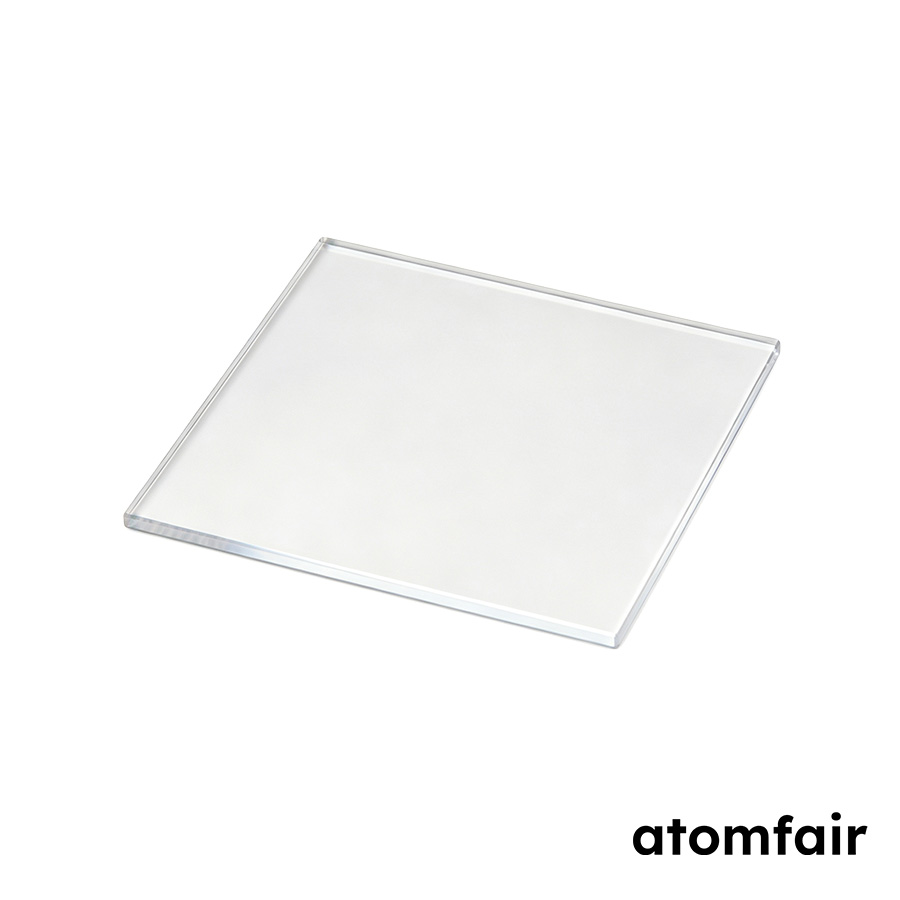
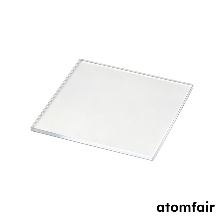
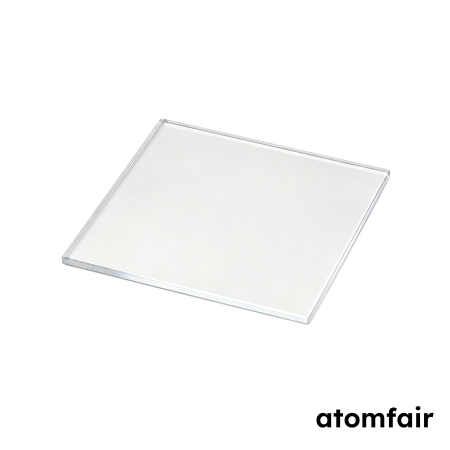
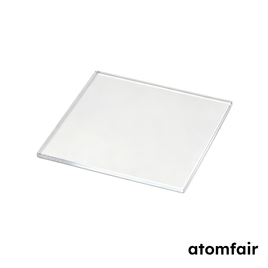
Quartz glass Substrate – 2 inch (50.8 mm), 25 pcs/box
Product Type: Glass substrate
Research-grade laboratory product
|
|||||||||||||||||||||||||||
|
|||||||||||||||||||||||||||
|
PRODUCT SELECTION SUPPORT
For model selection, material matching or specification support, contact our technical sales team.
E-MAIL: inquiry@atomfair.com
|
|||||||||||||||||||||||||||
|
Manufacturer: Atomfair LLC
Brand: ATOMFAIR®
|
This substrate exhibits low roughness and high surface quality, making it susceptible to particulate contamination and scratch damage during handling. Environmental moisture or improper storage may degrade surface finish and optical performance.
- Surface contamination risk: Contaminants such as dust, oils, or residues can compromise the specified Ra <0.5 nm roughness and Scratch/Dig 40/20 surface quality.
- Scratch and dig sensitivity: Mechanical contact with hard or abrasive surfaces risks introducing scratches or digs that exceed the stated 40/20 specification.
- Storage environment requirement: Store substrates in a clean, dry, low-particulate environment to preserve optical quality and prevent surface degradation.
Proper handling of quartz glass substrates minimizes contamination and surface damage that could affect optical performance. Follow these steps for inspection and transfer using appropriate tools.
Required Equipment: Cleanroom-grade gloves, PTFE-coated tweezers or vacuum wand, Lint-free wipes, Optical microscope or inspection station
- Don clean gloves
Inspect your gloves for residues or tears before touching any substrate to avoid oil or particle transfer. - Remove substrate from box
Use PTFE-coated tweezers or a vacuum wand to lift the substrate by its edge, never contacting the optical surfaces. - Inspect surface quality
Examine the substrate under an optical microscope to verify the absence of contamination or scratches beyond the Scratch/Dig 40/20 specification. - Place substrate into storage or holder
Transfer the substrate to a clean container or padded holder, ensuring it rests flat without edge chipping or surface contact.
What is the typical thickness tolerance for the 2-inch quartz glass substrate, and how does it affect optical path length consistency?
The typical thickness is 500 µm with a tolerance of ±25 µm, as specified in the technical data. This tight tolerance ensures consistent optical path length across substrates, which is critical for applications such as interferometry, spectroscopy, or multi-layer thin-film deposition where phase uniformity is required.
How does the 16 mm flat length or notch orientation affect alignment in standard wafer handling equipment?
The substrate includes a 16 mm flat (or notch) as stated in the specifications, which conforms to the SEMI standard for 2-inch wafers. This feature enables precise orientation alignment in automated wafer handlers, cassette systems, and photolithography tools, ensuring repeatable positioning during processing.
What are the implications of the <5 µm flatness specification for bonding or mounting applications?
The <5 µm flatness specification ensures minimal substrate warpage, which is essential for achieving uniform contact in thermal bonding, vacuum chuck mounting, or when used as a reference surface in optical assemblies. This level of flatness reduces stress-induced distortion and improves yield in processes like wafer-level packaging or precision alignment.
This 2-inch quartz glass substrate (AF-WF-S-GLAS-02IN-G070) offers a surface roughness of Ra <0.5 nm, flatness <5 µm, and Scratch/Dig 40/20 quality, making it suitable for demanding optical and thin-film applications where substrate uniformity is critical.
Positive
- Ultra-low surface roughness: Ra <0.5 nm roughness minimizes scattering losses and ensures high-quality film deposition or optical performance in precision coating and photonics applications.
- Tight flatness and surface quality: <5 µm flatness and Scratch/Dig 40/20 specification provide consistent substrate geometry and defect control, critical for lithography, interferometry, and semiconductor processing.
Trade-offs
- Thin substrate handling fragility: At 500 ±25 µm thickness, the substrate is mechanically delicate and requires careful handling with vacuum chucks or edge-gripping tools to avoid breakage during processing.
- Fixed format limits flexibility: Supplied only in 2-inch diameter with a 16 mm flat length; users requiring other sizes or custom notches must select alternative models, potentially increasing lead time or inventory complexity.
Every advanced material, component, equipment, and instrument in our catalog is backed by rigorous testing. We maintain strict internal quality management frameworks and align with CE conformity metrics to deliver transparent, reproducible performance data via our public open-science repository.
To request raw batch performance data, submit formal vendor registration paperwork, or execute a fast-turnaround R&D manufacturing loop, contact us at inquiry@atomfair.com.
Item is dispatched under the Atomfair Shipping & Delivery Framework (Free worldwide shipping on orders over $59 USD excl. heavy equipment). Return is governed by the Atomfair Return & Refund Policy (7-day technical return window).